
Product Specifications


CY8C29466/CY8C29566
CY8C29666/CY8C29866
Document Number: 38-12013 Rev. AB Page 23 of 67
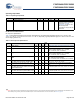
DC GPIO Specifications
Tab le 14 lists guaranteed maximum and minimum specifications for the voltage and temperature ranges: 4.75 V to 5.25 V and
–40 °C T
A
85 °C, or 3.0 V to 3.6 V and –40 °C T
A
85 °C, respectively. Typical parameters apply to 5 V and 3.3 V at 25 °C and
are for design guidance only.
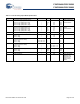
Table 14. DC GPIO Specifications
Symbol Description Min Typ Max Unit Notes
R
PU
Pull-up resistor 4 5.6 8 k
R
PD
Pull-down resistor 4 5.6 8 k
V
OH
High output level V
DD
– 1.0 – – V I
OH
= 10 mA, V
DD
= 4.75 to 5.25 V (8 total loads,
4 on even port pins (for example, P0[2], P1[4]),
4 on odd port pins (for example, P0[3], P1[5])).
80 mA maximum combined I
OH
budget.
V
OL
Low output level – – 0.75 V I
OL
= 25 mA, V
DD
= 4.75 to 5.25 V (8 total loads,
4 on even port pins (for example, P0[2], P1[4]),
4 on odd port pins (for example, P0[3], P1[5])).
150 mA maximum combined I
OL
budget.
I
OH
High level source current 10 – – mA V
OH
= V
DD
– 1.0 V, see the limitations of the total
current in the note for V
OH
I
OL
Low level sink current 25 – – mA V
OL
= 0.75 V, see the limitations of the total
current in the note for V
OL
V
IL
Input low level – – 0.8 V V
DD
= 3.0 to 5.25
V
IH
Input high level 2.1 – – V V
DD
= 3.0 to 5.25
V
H
Input hysteresis – 60 – mV
I
IL
Input leakage (absolute value) – 1 – nA Gross tested to 1 µA.
C
IN
Capacitive load on pins as input – 3.5 10 pF Package and pin dependent. Temp = 25 °C.
C
OUT
Capacitive load on pins as output – 3.5 10 pF Package and pin dependent. Temp = 25 °C.