
Product Specifications


CY8C29466/CY8C29566
CY8C29666/CY8C29866
Document Number: 38-12013 Rev. AB Page 22 of 67
Operating Temperature
DC Electrical Characteristics
DC Chip-Level Specifications
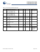
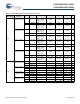
Tab le 13 lists guaranteed maximum and minimum specifications for the voltage and temperature ranges: 4.75 V to 5.25 V and
–40 °C T
A
85 °C, or 3.0 V to 3.6 V and –40 °C T
A
85 °C, respectively. Typical parameters apply to 5 V and 3.3 V at 25 °C and
are for design guidance only.
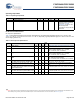
Table 12. Operating Temperature
Symbol Description Min Typ Max Unit Notes
T
A
Ambient temperature –40 – +85 °C
T
J
Junction temperature –40 – +100 °C The temperature rise from
ambient to junction is package
specific. See “Thermal
Impedances” on page 51. You
must limit the power
consumption to comply with this
requirement.
Table 13. DC Chip-Level Specifications
Symbol Description Min Typ Max
Unit
s
Notes
V
DD
[14]
Supply voltage 3.00 – 5.25 V See DC POR, SMP, and LVD Specifications on page
36.
I
DD
Supply current – 8 14 mA Conditions are 5.0 V, T
A
= 25 °C, CPU = 3 MHz,
SYSCLK doubler disabled, VC1 = 1.5 MHz,
VC2 = 93.75 kHz, VC3 = 0.366 kHz.
I
DD3
Supply current – 5 9 mA Conditions are V
DD
= 3.3 V, T
A
= 25 °C, CPU = 3 MHz,
SYSCLK doubler disabled, VC1 = 1.5 MHz,
VC2 = 93.75 kHz, VC3 = 0.366 kHz.
I
DDP
Supply current when IMO = 6 MHz using SLIMO
mode.
– 2 3 mA Conditions are V
DD
= 3.3 V, T
A
= 25 °C, CPU = 0.75
MHz, SYSCLK doubler disabled,
VC1 = 0.375 MHz, VC2 = 23.44 kHz, VC3 = 0.09 kHz.
I
SB
Sleep (Mode) current with POR, LVD, sleep
timer, WDT, and internal slow oscillator active.
– 3 10 µA Conditions are with internal slow speed oscillator,
V
DD
= 3.3 V, –40
C T
A
55 °C.
I
SBH
Sleep (Mode) current with POR, LVD, sleep
timer, WDT, and internal slow oscillator active.
– 4 25 µA Conditions are with internal slow speed oscillator,
V
DD
= 3.3 V, 55
°C < T
A
85 °C.
I
SBXTL
Sleep (Mode) current with POR, LVD, sleep
timer, WDT, internal slow oscillator, and 32 kHz
crystal oscillator active.
– 4 12 µA Conditions are with properly loaded, 1 µW max,
32.768 kHz crystal. V
DD
= 3.3 V, –40 °C T
A
55 °C.
I
SBXTLH
Sleep (Mode) current with POR, LVD, sleep
timer, WDT, and 32 kHz crystal oscillator active.
– 5 27 µA Conditions are with properly loaded, 1 µW max,
32.768 kHz crystal. V
DD
= 3.3 V, 55 °C < T
A
85 °C.
V
REF
Reference voltage (Bandgap) 1.28 1.3 1.32 V Trimmed for appropriate V
DD
.
Note
14. Errata: When V
DD
of the device is pulled below ground just before power-on; the first read from each 8K Flash bank may be corrupted apart from flash bank 0. This
an be solved by doing a dummy read from each flash bank prior to use of the Flash banks. For more information, see Errata on page 61.