
Product Specifications


CY8C29466/CY8C29566
CY8C29666/CY8C29866
Document Number: 38-12013 Rev. AB Page 16 of 67
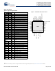
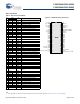
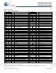
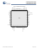
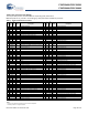
100-Pin Part Pinout (On-Chip Debug)
The 100-pin TQFP part is for the CY8C29000 On-Chip Debug (OCD) PSoC device.
Note OCD parts are only used for in-circuit debugging. OCD parts are NOT available for production.
Table 7. 100-Pin OCD Part Pinout (TQFP)
Pin
No.
Digital
Analog
Name Description
Pin
No.
Digital
Analog
Name Description
1 NC No internal connection 51 NC No internal connection
2 NC No internal connection 52 I/O P5[0]
3 I/O I P0[1] Analog column mux input 53 I/O P5[2]
4 I/O P2[7] 54 I/O P5[4]
5 I/O P2[5] 55 I/O P5[6]
6 I/O I P2[3] Direct switched capacitor block input 56 I/O P3[0]
7 I/O I P2[1] Direct switched capacitor block input 57 I/O P3[2]
8 I/O P4[7] 58 I/O P3[4]
9 I/O P4[5] 59 I/O P3[6]
10 I/O P4[3] 60 HCLK OCD high speed clock output
11 I/O P4[1] 61 CCLK OCD CPU clock output
12 OCDE OCD even data I/O 62 Input XRES Active high pin reset with internal pull-down
13 OCDO OCD odd data output 63 I/O P4[0]
14 Power SMP Switch Mode Pump (SMP) connection to required
external components
64 I/O P4[2]
15 Power V
SS
Ground connection
[12]
65 Power V
SS
Ground connection
[12]
16 I/O P3[7] 66 I/O P4[4]
17 I/O P3[5] 67 I/O P4[6]
18 I/O P3[3] 68 I/O I P2[0] Direct switched capacitor block input
19 I/O P3[1] 69 I/O I P2[2] Direct switched capacitor block input
20 I/O P5[7] 70 I/O P2[4] External Analog Ground (AGND) input
21 I/O P5[5] 71 NC No internal connection
22 I/O P5[3] 72 I/O P2[6] External Voltage Reference (VREF) input
23 I/O P5[1] 73 NC No internal connection
24 I/O P1[7] I
2
C SCL 74 I/O I P0[0] Analog column mux input
25 NC No internal connection 75 NC No internal connection
26 NC No internal connection 76 NC No internal connection
27 NC No internal connection 77 I/O I/O P0[2] Analog column mux input and column output
28 I/O P1[5] I
2
C SDA 78 NC No internal connection
29 I/O P1[3] I
FMTEST
79 I/O I/O P0[4] Analog column mux input and column output, V
REF
30 I/O P1[1]
[13]
Crystal (XTALin), I
2
C SCL, TC SCLK. 80 NC No internal connection
31 NC No internal connection 81 I/O I P0[6] Analog column mux input
32 Power V
DD
Supply voltage 82 Power V
DD
Supply voltage
33 NC No internal connection 83 Power V
DD
Supply voltage
34 Power V
SS
Ground connection
[12]
84 Power V
SS
Ground connection
[12]
35 NC No internal connection 85 Power V
SS
Ground connection
[12]
36 I/O P7[7] 86 I/O P6[0]
37 I/O P7[6] 87 I/O P6[1]
38 I/O P7[5] 88 I/O P6[2]
39 I/O P7[4] 89 I/O P6[3]
40 I/O P7[3] 90 I/O P6[4]
41 I/O P7[2] 91 I/O P6[5]
42 I/O P7[1] 92 I/O P6[6]
43 I/O P7[0] 93 I/O P6[7]
44 I/O P1[0]* Crystal (XTALout), I
2
C SDA, TC SDATA 94 NC No internal connection
45 I/O P1[2] V
FMTEST
95 I/O I P0[7] Analog column mux input
46 I/O P1[4] Optional External Clock Input (EXTCLK) 96 NC No internal connection
47 I/O P1[6] 97 I/O I/O P0[5] Analog column mux input and column output
48 NC No internal connection 98 NC No internal connection
49 NC No internal connection 99 I/O I/O P0[3] Analog column mux input and column output
50 NC No internal connection 100 NC No internal connection
LEGEND A = Analog, I = Input, O = Output, NC = No connection. Pin must be left floating, TC/TM: Test.
Notes
12. All V
SS
pins should be brought out to one common GND plane.
13. ISSP pin which is not High-Z at POR.