
Product Specifications


CY8C29466/CY8C29566
CY8C29666/CY8C29866
Document Number: 38-12013 Rev. AB Page 14 of 67
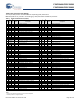
100-Pin Part Pinout
Table 6. 100-Pin Part Pinout (TQFP)
Pin
No.
Type
Name Description
Pin
No.
Type
Name Description
Digital Analog Digital Analog
1 NC No connection. Pin must be left floating 51 NC No connection. Pin must be left floating
2 NC No connection. Pin must be left floating 52 I/O P5[0]
3 I/O I P0[1] Analog column mux input 53 I/O P5[2]
4 I/O P2[7] 54 I/O P5[4]
5 I/O P2[5] 55 I/O P5[6]
6 I/O I P2[3] Direct switched capacitor block input 56 I/O P3[0]
7 I/O I P2[1] Direct switched capacitor block input 57 I/O P3[2]
8 I/O P4[7] 58 I/O P3[4]
9 I/O P4[5] 59 I/O P3[6]
10 I/O P4[3] 60 NC No connection. Pin must be left floating
11 I/O P4[1] 61 NC No connection. Pin must be left floating
12 NC No connection. Pin must be left floating 62 Input XRES Active high external reset with internal
pull-down
13 NC No connection. Pin must be left floating 63 I/O P4[0]
14 Power SMP Switch mode pump (SMP) connection to
external components required
64 I/O P4[2]
15 Power V
SS
Ground connection
[10]
65 Power V
SS
Ground connection
[10]
16 I/O P3[7] 66 I/O P4[4]
17 I/O P3[5] 67 I/O P4[6]
18 I/O P3[3] 68 I/O I P2[0] Direct switched capacitor block input
19 I/O P3[1] 69 I/O I P2[2] Direct switched capacitor block input
20 I/O P5[7] 70 I/O P2[4] External Analog Ground (AGND)
21 I/O P5[5] 71 NC No connection. Pin must be left floating
22 I/O P5[3] 72 I/O P2[6] External Voltage Reference (VREF)
23 I/O P5[1] 73 NC No connection. Pin must be left floating
24 I/O P1[7] I
2
C SCL 74 I/O I P0[0] Analog column mux input
25 NC No connection. Pin must be left floating 75 NC No connection. Pin must be left floating
26 NC No connection. Pin must be left floating 76 NC No connection. Pin must be left floating
27 NC No connection. Pin must be left floating 77 I/O I/O P0[2] Analog column mux input and column output
28 I/O P1[5] I
2
C SDA 78 NC No connection. Pin must be left floating
29 I/O P1[3] 79 I/O I/O P0[4] Analog column mux input and column output
30 I/O P1[1] Crystal (XTALin), I
2
C Serial Clock (SCL),
ISSP-SCLK
[11]
80 NC No connection. Pin must be left floating
31 NC No connection. Pin must be left floating 81 I/O I P0[6] Analog column mux input
32 Power V
DD
Supply voltage 82 Power V
DD
Supply voltage
33 NC No connection. Pin must be left floating 83 Power V
DD
Supply voltage
34 Power V
SS
Ground connection
[10]
84 Power V
SS
Ground connection
[10]
35 NC No connection. Pin must be left floating 85 Power V
SS
Ground connection
[10]
36 I/O P7[7] 86 I/O P6[0]
37 I/O P7[6] 87 I/O P6[1]
38 I/O P7[5] 88 I/O P6[2]
39 I/O P7[4] 89 I/O P6[3]
40 I/O P7[3] 90 I/O P6[4]
41 I/O P7[2] 91 I/O P6[5]
42 I/O P7[1] 92 I/O P6[6]
43 I/O P7[0] 93 I/O P6[7]
44 I/O P1[0] Crystal (XTALout), I
2
C Serial Data (SDA),
ISSP-SDATA
[11]
94 NC No connection. Pin must be left floating
45 I/O P1[2] 95 I/O I P0[7] Analog column mux input
46 I/O P1[4] Optional EXTCLK 96 NC No connection. Pin must be left floating
47 I/O P1[6] 97 I/O I/O P0[5] Analog column mux input and column output
48 NC No connection. Pin must be left floating 98 NC No connection. Pin must be left floating
49 NC No connection. Pin must be left floating 99 I/O I/O P0[3] Analog column mux input and column output
50 NC No connection. Pin must be left floating 100 NC No connection. Pin must be left floating
LEGEND: A = Analog, I = Input, and O = Output.
Notes
10. All V
SS
pins should be brought out to one common GND plane.
11. These are the ISSP pins, which are not High Z at POR. See the
PSoC Programmable System-on-Chip Technical Reference Manual for details.