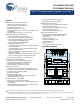
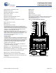
CY8C29466/CY8C29566 CY8C29666/CY8C29866 PSoC® Programmable System-on-Chip™ PSoC® Programmable System-on-Chip™ Features ■ ■ ■ ■ ■ ❐ Powerful Harvard-architecture processor ❐ M8C processor speeds to 24 MHz ❐ Two 8 × 8 multiply, 32-bit accumulate ❐ Low power at high speed ❐ Operating voltage: 3.0 V to 5.25 V ❐ Operating voltages down to 1.
CY8C29466/CY8C29566 CY8C29666/CY8C29866 More Information Note: For CY8C29X66 devices related Development Kits please click here. Cypress provides a wealth of data at www.cypress.com to help you to select the right PSoC device for your design, and to help you to quickly and effectively integrate the device into your design. For a comprehensive list of resources, see the knowledge base article “How to Design with PSoC® 1, PowerPSoC®, and PLC – KBA88292”.
CY8C29466/CY8C29566 CY8C29666/CY8C29866 Contents PSoC Functional Overview .............................................. 4 PSoC Core .................................................................. 4 Digital System ............................................................. 4 Analog System ............................................................ 5 Additional System Resources ..................................... 6 PSoC Device Characteristics ......................................
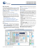
CY8C29466/CY8C29566 CY8C29666/CY8C29866 The digital system is composed of 16 digital PSoC blocks. Each block is an 8-bit resource that can be used alone or combined with other blocks to form 8-, 16-, 24-, and 32-bit peripherals, which are called user modules. Figure 2.
CY8C29466/CY8C29566 CY8C29666/CY8C29866 Digital peripheral configurations include: ■ DTMF Dialer ■ PWMs (8- and 16-bit) ■ Modulators ■ PWMs with dead band (8- and 16-bit) ■ Correlators ■ Counters (8- to 32-bit) ■ Peak detectors ■ Timers (8- to 32-bit) ■ Many other topologies possible ■ UART 8-bit with selectable parity (up to 2) ■ SPI slave and master (up to 2) Analog blocks are provided in columns of three, which includes one continuous time (CT) and two switched capacitor (SC) block
CY8C29466/CY8C29566 CY8C29666/CY8C29866 Additional System Resources System resources, some of which were previously listed, provide additional capability useful to complete systems. Additional resources include a multiplier, decimator, switch mode pump, low-voltage detection, and power-on-reset (POR). ■ ■ The decimator provides a custom hardware filter for digital signal processing applications including the creation of delta sigma ADCs.
CY8C29466/CY8C29566 CY8C29666/CY8C29866 Development Tools PSoC Designer™ is the revolutionary Integrated Design Environment (IDE) that you can use to customize PSoC to meet your specific application requirements. PSoC Designer software accelerates system design and time to market. Develop your applications using a library of precharacterized analog and digital peripherals (called user modules) in a drag-and-drop design environment.
CY8C29466/CY8C29566 CY8C29666/CY8C29866 Designing with PSoC Designer The development process for the PSoC® device differs from that of a traditional fixed function microprocessor. The configurable analog and digital hardware blocks give the PSoC architecture a unique flexibility that pays dividends in managing specification change during development and by lowering inventory costs. These configurable resources, called PSoC Blocks, have the ability to implement a wide variety of user-selectable functions.
CY8C29466/CY8C29566 CY8C29666/CY8C29866 Organize and Connect You build signal chains at the chip level by interconnecting user modules to each other and the I/O pins. You perform the selection, configuration, and routing so that you have complete control over all on-chip resources. Generate, Verify, and Debug When you are ready to test the hardware configuration or move on to developing code for the project, you perform the “Generate Configuration Files” step.
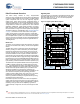
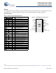
CY8C29466/CY8C29566 CY8C29666/CY8C29866 Pinouts The CY8C29x66 PSoC device is available in a variety of packages which are listed and illustrated in the following tables. Every port pin (labeled with a “P”) is capable of Digital I/O. However, VSS, VDD, SMP, and XRES are not capable of Digital I/O. 28-Pin Part Pinout Table 2. 28-Pin Part Pinout (PDIP, SSOP, SOIC) Pin No.
CY8C29466/CY8C29566 CY8C29666/CY8C29866 44-Pin Part Pinout Table 3.
CY8C29466/CY8C29566 CY8C29666/CY8C29866 48-Pin Part Pinout Table 4. 48-Pin Part Pinout (SSOP) Pin No.
CY8C29466/CY8C29566 CY8C29666/CY8C29866 Table 5.
CY8C29466/CY8C29566 CY8C29666/CY8C29866 100-Pin Part Pinout Table 6. 100-Pin Part Pinout (TQFP) Pin No.
CY8C29466/CY8C29566 CY8C29666/CY8C29866 VDD VDD P0[6], A, I NC P0[4], A, IO NC P0[2], A, IO NC 87 86 85 84 83 82 81 80 79 78 77 76 P6[7] P6[6] P6[5] P6[4] P6[3] P6[2] P6[1] P6[0] VSS VSS TQFP Document Number: 38-12013 Rev.
CY8C29466/CY8C29566 CY8C29666/CY8C29866 100-Pin Part Pinout (On-Chip Debug) The 100-pin TQFP part is for the CY8C29000 On-Chip Debug (OCD) PSoC device. Note OCD parts are only used for in-circuit debugging. OCD parts are NOT available for production.
CY8C29466/CY8C29566 CY8C29666/CY8C29866 77 76 P6[0] VSS VSS VDD VDD P0[6], AI NC P0[4], AIO NC P0[2], AIO NC 87 86 85 84 83 82 81 80 79 78 90 89 88 P6[7] P6[6] P6[5] P6[4] P6[3] P6[2] P6[1] 98 97 96 95 94 93 92 91 75 74 73 72 71 70 69 68 67 66 65 64 63 62 61 60 59 58 57 56 55 OCD TQFP NC P0[0] , AI NC P2[6] , External VREF NC P2[4] , External AGND P2[2] , AI P2[0] , AI P4[6] P4[4] VSS P4[2] P4[0] XRES CCLK HCLK P3[6] P3[4] P3[2] P3[0] P5[6] P5[4] P5[2] P5[0] NC NC NC XTALout, I2C SDA, P1[0] P1[2]
CY8C29466/CY8C29566 CY8C29666/CY8C29866 Register Reference This section lists the registers of the CY8C29x66 PSoC device. For detailed register information, refer to the PSoC Programmable System-on-Chip Technical Reference Manual. Register Conventions The register conventions specific to this section are listed in Table 8. Table 8.
CY8C29466/CY8C29566 CY8C29666/CY8C29866 Table 9.
CY8C29466/CY8C29566 CY8C29666/CY8C29866 Table 10.
CY8C29466/CY8C29566 CY8C29666/CY8C29866 Electrical Specifications This section presents the DC and AC electrical specifications of the CY8C29x66 PSoC device. For the most up-to-date electrical specifications, confirm that you have the most recent datasheet by going to the web at http://www.cypress.com. Specifications are valid for –40 °C TA 85 °C and TJ 100 °C, except where noted. Refer to Table 29 for the electrical specifications on the internal main oscillator (IMO) using SLIMO mode. Figure 10.
CY8C29466/CY8C29566 CY8C29666/CY8C29866 Operating Temperature Table 12. Operating Temperature Symbol TA TJ Description Ambient temperature Junction temperature Min –40 –40 Typ – – Max +85 +100 Unit °C °C Notes The temperature rise from ambient to junction is package specific. See “Thermal Impedances” on page 51. You must limit the power consumption to comply with this requirement.
CY8C29466/CY8C29566 CY8C29666/CY8C29866 DC GPIO Specifications Table 14 lists guaranteed maximum and minimum specifications for the voltage and temperature ranges: 4.75 V to 5.25 V and –40 °C TA 85 °C, or 3.0 V to 3.6 V and –40 °C TA 85 °C, respectively. Typical parameters apply to 5 V and 3.3 V at 25 °C and are for design guidance only. Table 14. DC GPIO Specifications Symbol Description Min Typ Max Unit 4 5.6 8 k Pull-down resistor 4 5.6 8 k High output level VDD – 1.
CY8C29466/CY8C29566 CY8C29666/CY8C29866 DC Operational Amplifier Specifications Table 15 and Table 16 list guaranteed maximum and minimum specifications for the voltage and temperature ranges: 4.75 V to 5.25 V and –40 °C TA 85 °C, or 3.0 V to 3.6 V and –40 °C TA 85 °C, respectively. Typical parameters apply to 5 V and 3.3 V at 25 °C and are for design guidance only. The Operational Amplifier is a component of both the Analog Continuous Time PSoC blocks and the Analog Switched Cap PSoC blocks.
CY8C29466/CY8C29566 CY8C29666/CY8C29866 Table 16. 3.3-V DC Operational Amplifier Specifications Symbol Description Min Typ Max Unit VOSOA Input offset voltage (absolute value) Power = Low, Opamp bias = Low Power = Low, Opamp bias = High Power = Medium, Opamp bias = Low Power = Medium, Opamp bias = High Power = High, Opamp bias = Low Power = High, Opamp bias = High – – – – – – 1.4 1.4 1.4 1.4 1.
CY8C29466/CY8C29566 CY8C29666/CY8C29866 DC Analog Output Buffer Specifications Table 18 and Table 19 list guaranteed maximum and minimum specifications for the voltage and temperature ranges: 4.75 V to 5.25 V and –40 °C TA 85 °C, or 3.0 V to 3.6 V and –40 °C TA 85 °C, respectively. Typical parameters apply to 5 V and 3.3 V at 25 °C and are for design guidance only. Table 18.
CY8C29466/CY8C29566 CY8C29666/CY8C29866 Table 19. 3.3-V DC Analog Output Buffer Specifications Symbol Description Min Typ Max Unit VOSOB Input offset voltage (absolute value) Power = Low, Opamp bias = Low Power = Low, Opamp bias = High Power = High, Opamp bias = Low Power = High, Opamp bias = High – – – – 3.2 3.
CY8C29466/CY8C29566 CY8C29666/CY8C29866 DC Switch Mode Pump Specifications Table 20 lists guaranteed maximum and minimum specifications for the voltage and temperature ranges: 4.75 V to 5.25 V and –40 °C TA 85 °C, or 3.0 V to 3.6 V and –40 °C TA 85 °C, respectively. Typical parameters apply to 5 V and 3.3 V at 25 °C and are for design guidance only. Table 20. DC Switch Mode Pump (SMP) Specifications Min Typ Max Unit Notes VPUMP 5 V Symbol 5 V output voltage at VDD from pump Description 4.
CY8C29466/CY8C29566 CY8C29666/CY8C29866 Figure 12. Basic Switch Mode Pump Circuit D1 Vdd L1 V BAT + V PUMP C1 SMP Battery PSoC Vss DC Analog Reference Specifications The following tables list guaranteed maximum and minimum specifications for the voltage and temperature ranges: 4.75 V to 5.25 V and –40 °C TA 85 °C, or 3.0 V to 3.6 V and –40 °C TA 85 °C, respectively. Typical parameters apply to 5 V and 3.3 V at 25 °C and are for design guidance only.
CY8C29466/CY8C29566 CY8C29666/CY8C29866 Table 21.
CY8C29466/CY8C29566 CY8C29666/CY8C29866 Table 21.
CY8C29466/CY8C29566 CY8C29666/CY8C29866 Table 21.
CY8C29466/CY8C29566 CY8C29666/CY8C29866 Table 22. 3.3-V DC Analog Reference Specifications Reference ARF_CR[5:3] Reference Power Settings RefPower = High Opamp bias = High RefPower = High Opamp bias = Low 0b000 RefPower = Med Opamp bias = High RefPower = Med Opamp bias = Low RefPower = High Opamp bias = High Symbol Reference Description Min Typ Max Unit VDD/2 + BandGap VDD/2 + 1.225 VDD/2 + 1.292 VDD/2 + 1.361 V VDD/2 VDD/2 – 0.067 VDD/2 – 0.002 VDD/2 + 0.
CY8C29466/CY8C29566 CY8C29666/CY8C29866 Table 22. 3.3-V DC Analog Reference Specifications (continued) Reference ARF_CR[5:3] Reference Power Settings RefPower = High Opamp bias = High RefPower = High Opamp bias = Low 0b010 RefPower = Med Opamp bias = High RefPower = Med Opamp bias = Low Symbol Reference Description Min Typ Max Unit VDD – 0.06 VDD – 0.010 VDD V VDD/2 – 0.05 VDD/2 – 0.002 VDD/2 + 0.040 V VREFHI Ref High VAGND AGND VREFLO Ref Low Vss Vss Vss + 0.009 Vss + 0.
CY8C29466/CY8C29566 CY8C29666/CY8C29866 Table 22. 3.3-V DC Analog Reference Specifications (continued) Reference ARF_CR[5:3] Reference Power Settings RefPower = High Opamp bias = High RefPower = High Opamp bias = Low 0b110 RefPower = Med Opamp bias = High RefPower = Med Opamp bias = Low Symbol Reference VREFHI Ref High VAGND AGND Min Typ Max Unit 2 × BandGap 2.507 2.598 2.698 V BandGap 1.203 1.307 1.424 V Vss Vss + 0.012 Vss + 0.
CY8C29466/CY8C29566 CY8C29666/CY8C29866 DC POR, SMP, and LVD Specifications The following table lists guaranteed maximum and minimum specifications for the voltage and temperature ranges: 4.75 V to 5.25 V and –40 °C TA 85 °C, or 3.0 V to 3.6 V and –40 °C TA 85 °C, respectively. Typical parameters apply to 5 V and 3.3 V at 25 °C and are for design guidance only. Table 26.
CY8C29466/CY8C29566 CY8C29666/CY8C29866 DC Programming Specifications The following table lists guaranteed maximum and minimum specifications for the voltage and temperature ranges: 4.75 V to 5.25 V and –40 °C TA 85 °C, or 3.0 V to 3.6 V and –40 °C TA 85 °C, respectively. Typical parameters apply to 5 V and 3.3 V at 25 °C and are for design guidance only. Table 27. DC Programming Specifications Symbol VDDP VDDLV VDDHV Description Min Typ Units Notes 4.5 5 5.
CY8C29466/CY8C29566 CY8C29666/CY8C29866 AC Electrical Characteristics AC Chip-Level Specifications The following table lists guaranteed maximum and minimum specifications for the voltage and temperature ranges: 4.75 V to 5.25 V and –40 °C TA 85 °C, or 3.0 V to 3.6 V and –40 °C TA 85 °C, respectively. Typical parameters apply to 5 V and 3.3 V at 25 °C and are for design guidance only. Note See the individual user module datasheets for information on maximum frequencies for user modules. Table 29.
CY8C29466/CY8C29566 CY8C29666/CY8C29866 Table 29. AC Chip-Level Specifications (continued) Min Typ Max Units SRPOWER_UP Symbol Power supply slew rate – – 250 TPOWERUP [25] Time from end of POR to CPU executing code – 16 100 V/ms VDD slew rate during power-up ms Power-up from 0 V.
CY8C29466/CY8C29566 CY8C29666/CY8C29866 AC General Purpose I/O Specifications The following table lists guaranteed maximum and minimum specifications for the voltage and temperature ranges: 4.75 V to 5.25 V and –40 °C TA 85 °C, or 3.0 V to 3.6 V and –40 °C TA 85 °C, respectively. Typical parameters apply to 5 V and 3.3 V at 25 °C and are for design guidance only. Table 30.
CY8C29466/CY8C29566 CY8C29666/CY8C29866 Table 32. 3.3-V AC Operational Amplifier Specifications Symbol tROA tSOA SRROA SRFOA BWOA ENOA Description Rising settling time to 0.1% of a 1 V Step (10 pF load, unity gain) Power = Low, Opamp bias = Low Power = Medium, Opamp bias = High Falling settling time to 0.
CY8C29466/CY8C29566 CY8C29666/CY8C29866 Analog Reference Noise spectrum: When bypassed by a capacitor on P2[4], the noise of the analog ground signal distributed to each block is reduced by a factor of up to 5 (14 dB). This is at frequencies above the corner frequency defined by the on-chip 8.1 K resistance and the external capacitor. Figure 18. Typical AGND Noise with P2[4] Bypass AGND = 1.
CY8C29466/CY8C29566 CY8C29666/CY8C29866 AC Digital Block Specifications The following table lists guaranteed maximum and minimum specifications for the voltage and temperature ranges: 4.75 V to 5.25 V and –40 °C TA 85 °C, or 3.0 V to 3.6 V and –40 °C TA 85 °C, respectively. Typical parameters apply to 5 V and 3.3 V at 25 °C and are for design guidance only. Table 34. AC Digital Block Specifications Function All functions Timer Description Min Typ Max Unit VDD 4.75 V – – 50.
CY8C29466/CY8C29566 CY8C29666/CY8C29866 AC Analog Output Buffer Specifications The following tables list guaranteed maximum and minimum specifications for the voltage and temperature ranges: 4.75 V to 5.25 V and –40 °C TA 85 °C, or 3.0 V to 3.6 V and –40 °C TA 85 °C, respectively. Typical parameters apply to 5 V and 3.3 V at 25 °C and are for design guidance only. Table 35. 5-V AC Analog Output Buffer Specifications Symbol tROB tSOB SRROB SRFOB BWOB BWOB Description Rising settling time to 0.
CY8C29466/CY8C29566 CY8C29666/CY8C29866 Table 38. 3.3-V AC External Clock Specifications Symbol Min Typ Max Unit Frequency with CPU clock divide by 1 0.093 – 12.3 MHz FOSCEXT Frequency with CPU clock divide by 2 or greater 0.186 – 24.6 MHz – High period with CPU clock divide by 1 41.7 – 5300 ns – Low period with CPU clock divide by 1 41.
CY8C29466/CY8C29566 CY8C29666/CY8C29866 AC I2C Specifications The following table lists guaranteed maximum and minimum specifications for the voltage and temperature ranges: 4.75 V to 5.25 V and –40 °C TA 85 °C, or 3.0 V to 3.6 V and –40 °C TA 85 °C, respectively. Typical parameters apply to 5 V and 3.3 V at 25 °C and are for design guidance only. Table 40.
CY8C29466/CY8C29566 CY8C29666/CY8C29866 Packaging Information This section illustrates the packaging specifications for the CY8C29x66 PSoC device, along with the thermal impedances for each package and the typical package capacitance on crystal pins. Important Note Emulation tools may require a larger area on the target PCB than the chip's footprint. For a detailed description of the emulation tools' dimensions, refer to the emulator pod drawings at http://www.cypress.com. Packaging Dimensions Figure 20.
CY8C29466/CY8C29566 CY8C29666/CY8C29866 Figure 21. 28-pin SSOP (210 Mils) Package Outline, 51-85079 51-85079 *F Figure 22. 28-pin SOIC (0.713 × 0.300 × 0.0932 Inches) Package Outline, 51-85026 51-85026 *H Document Number: 38-12013 Rev.
CY8C29466/CY8C29566 CY8C29666/CY8C29866 Figure 23. 44-pin TQFP (10 × 10 × 1.4 mm) Package Outline, 51-85064 51-85064 *F Figure 24. 48-pin SSOP (300 Mils) Package Outline, 51-85061 51-85061 *F Document Number: 38-12013 Rev.
CY8C29466/CY8C29566 CY8C29666/CY8C29866 Figure 25. 48-pin QFN (7 × 7 × 1.0 mm) 5.1 × 5.1 E-Pad (Sawn) Package Outline, 001-13191 001-13191 *H Figure 26. 100-pin TQFP (14 × 14 × 1.4 mm) Package Outline, 51-85048 51-85048 *I Important Note For information on the preferred dimensions for mounting the QFN packages, see the application note Design Guidelines for Cypress Quad Flat No Extended Lead (QFN) Packaged Devices – AN72845 available at http://www.cypress.com.
CY8C29466/CY8C29566 CY8C29666/CY8C29866 Thermal Impedances Capacitance on Crystal Pins Table 41. Thermal Impedances per Package Typical JA[ Package Table 42. Typical Package Capacitance on Crystal Pins 30] Package Package Capacitance 28-pin PDIP 69 °C/W 28-pin PDIP 3.5 pF 28-pin SSOP 94 °C/W 28-pin SSOP 2.8 pF 28-pin SOIC 67 °C/W 28-pin SOIC 2.7 pF 44-pin TQFP 60 °C/W 44-pin TQFP 2.6 pF 48-pin SSOP 69 °C/W 48-pin SSOP 3.3 pF 48-pin QFN[31] 28 °C/W 48-pin QFN 1.
CY8C29466/CY8C29566 CY8C29666/CY8C29866 Development Tool Selection This section presents the development tools available for all current PSoC device families including the CY8C29x66 family. Software PSoC Designer At the core of the PSoC development software suite is PSoC Designer, used to generate PSoC firmware applications. PSoC Designer is available free of charge at http://www.cypress.com and includes a free C compiler.
CY8C29466/CY8C29566 CY8C29666/CY8C29866 Device Programmers CY3207ISSP In-System Serial Programmer (ISSP) All device programmers can be purchased from the Cypress Online Store. The CY3207ISSP is a production programmer. It includes protection circuitry and an industrial case that is more robust than the MiniProg in a production-programming environment. CY3216 Modular Programmer The CY3216 Modular Programmer kit features a modular programmer and the MiniProg1 programming unit.
CY8C29466/CY8C29566 CY8C29666/CY8C29866 Ordering Information Flash (KB) RAM (KB) Switch Mode Pump Temperature Range Digital PSoC Blocks Analog PSoC Blocks Digital I/O Pins Analog Inputs Analog Outputs XRES Pin CY8C29466-24PXI CY8C29466-24PVXI 32 32 2 2 Yes Yes –40 °C to +85 °C –40 °C to +85 °C 16 16 12 12 24 24 12 12 4 4 Yes Yes CY8C29466-24PVXIT 32 2 Yes –40 °C to +85 °C 16 12 24 12 4 Yes CY8C29466-24SXI 32 2 Yes –40 °C to +85 °C 16 12 24 12 4 Yes CY8C29466-24SXI
CY8C29466/CY8C29566 CY8C29666/CY8C29866 Acronyms Table 45 lists the acronyms that are used in this document. Table 45.
CY8C29466/CY8C29566 CY8C29666/CY8C29866 Document Conventions Units of Measure Table 46 lists the unit sof measures. Table 46.
CY8C29466/CY8C29566 CY8C29666/CY8C29866 Glossary (continued) bias 1. A systematic deviation of a value from a reference value. 2. The amount by which the average of a set of values departs from a reference value. 3. The electrical, mechanical, magnetic, or other force (field) applied to a device to establish a reference level to operate the device. block 1. A functional unit that performs a single function, such as an oscillator. 2.
CY8C29466/CY8C29566 CY8C29666/CY8C29866 Glossary (continued) duty cycle The relationship of a clock period high time to its low time, expressed as a percent. emulator Duplicates (provides an emulation of) the functions of one system with a different system, so that the second system appears to behave like the first system. External Reset (XRES) An active high signal that is driven into the PSoC device. It causes all operation of the CPU and blocks to stop and return to a pre-defined state.
CY8C29466/CY8C29566 CY8C29666/CY8C29866 Glossary (continued) microcontroller An integrated circuit chip that is designed primarily for control systems and products. In addition to a CPU, a microcontroller typically includes memory, timing circuits, and IO circuitry. The reason for this is to permit the realization of a controller with a minimal quantity of chips, thus achieving maximal possible miniaturization. This in turn, reduces the volume and the cost of the controller.
CY8C29466/CY8C29566 CY8C29666/CY8C29866 Glossary (continued) shift register A memory storage device that sequentially shifts a word either left or right to output a stream of serial data. slave device A device that allows another device to control the timing for data exchanges between two devices. Or when devices are cascaded in width, the slave device is the one that allows another device to control the timing of data exchanges between the cascaded devices and an external interface.
CY8C29466/CY8C29566 CY8C29666/CY8C29866 Errata This section describes the errata for the PSoC Programmable System-on-Chip, CY8C29xxx family of devices. Details include errata trigger conditions, scope of impact, available workaround, and silicon revision applicability. Contact your local Cypress Sales Representative if you have questions.
CY8C29466/CY8C29566 CY8C29666/CY8C29866 // dummy read from each 8 K Flash bank // bank 1 mov A, 0x20 // MSB mov X, 0x00 // LSB romx // bank 2 mov A, 0x40 // MSB mov X, 0x00 // LSB romx // bank 3 mov A, 0x60 // MSB mov X, 0x00 // LSB romx // wait at least 5 µs mov X, 14 loop1: dec X jnz loop1 2. Internal main oscillator (IMO) tolerance deviation at temperature extremes ■ Problem Definition Asynchronous digital communications interfaces may fail framing beyond 0 to 70 °C.
CY8C29466/CY8C29566 CY8C29666/CY8C29866 Document History Page Document Title: CY8C29466/CY8C29566/CY8C29666/CY8C29866, PSoC® Programmable System-on-Chip™ Document Number: 38-12013 Revision ECN Origin of Change Submission Date ** 131151 New Silicon *A 132848 NWJ 01/21/2004 New information. First edition of preliminary datasheet. Description of Change 11/13/2003 New document (Revision **). *B 133205 NWJ 01/27/2004 Changed part numbers, increased SRAM data storage to 2 K bytes.
CY8C29466/CY8C29566 CY8C29666/CY8C29866 Document History Page (continued) Document Title: CY8C29466/CY8C29566/CY8C29666/CY8C29866, PSoC® Programmable System-on-Chip™ Document Number: 38-12013 Revision ECN Origin of Change *N 2902396 NJF 03/30/2010 Updated and content in Digital System Updated Cypress website links. Removed reference to PSoC Designer 4.
CY8C29466/CY8C29566 CY8C29666/CY8C29866 Document History Page (continued) Document Title: CY8C29466/CY8C29566/CY8C29666/CY8C29866, PSoC® Programmable System-on-Chip™ Document Number: 38-12013 Revision ECN Origin of Change Submission Date *V 3991993 PMAD 05/08/2013 Updated Packaging Information: spec 51-85014 – Changed revision from *F to *G. spec 51-85061 – Changed revision from *E to *F. spec 001-13191 – Changed revision from *F to *G.
CY8C29466/CY8C29566 CY8C29666/CY8C29866 Document History Page (continued) Document Title: CY8C29466/CY8C29566/CY8C29666/CY8C29866, PSoC® Programmable System-on-Chip™ Document Number: 38-12013 Revision ECN Origin of Change *Y 4461247 ASRI Submission Date Description of Change 07/30/2014 Replaced references of “Application Notes for Surface Mount Assembly of Amkor’s MicroLeadFrame (MLF) Packages” with “Design Guidelines for Cypress Quad Flat No Extended Lead (QFN) Packaged Devices – AN72845” in all in
CY8C29466/CY8C29566 CY8C29666/CY8C29866 Sales, Solutions, and Legal Information Worldwide Sales and Design Support Cypress maintains a worldwide network of offices, solution centers, manufacturer’s representatives, and distributors. To find the office closest to you, visit us at Cypress Locations. PSoC® Solutions Products Automotive Clocks & Buffers Interface Lighting & Power Control cypress.com/go/automotive cypress.com/go/clocks cypress.com/go/interface cypress.com/go/powerpsoc cypress.