
Data Sheet

PRELIMINARY
VS1063a Datasheet
4 CHARACTERISTICS & SPECIFICATIONS
4 Characteristics & Specifications
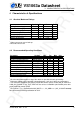
4.1 Absolute Maximum Ratings
Parameter Symbol Min Max Unit
Analog Positive Supply AVDD -0.3 3.6 V
Digital Positive Supply CVDD -0.3 1.85 V
I/O Positive Supply IOVDD -0.3 3.6 V
Current at Any Non-Power Pin
1
±50 mA
Voltage at Any Digital Input -0.3 IOVDD+0.3
2
V
Operating Temperature -30 +85
◦
C
Storage Temperature -65 +150
◦
C
1
Higher current can cause latch-up.
2
Must not exceed 3.6 V
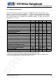
4.2 Recommended Operating Conditions
Parameter Symbol Min Typ Max Unit
Ambient Operating Temperature -30 +85
◦
C
Analog and Digital Ground
1
AGND DGND 0.0 V
Positive Analog, REF=1.23V AVDD 2.5 2.8 3.6 V
Positive Analog, REF=1.65V
2
AVDD 3.3 3.3 3.6 V
Positive Digital CVDD 1.7 1.8 1.85 V
I/O Voltage IOVDD 1.8 2.8 3.6 V
Input Clock Frequency
3
XTALI 12 12.288 13 MHz
Internal Clock Frequency CLKI 12 36.864 61.5 MHz
Internal Clock Multiplier
4
1.0× 3.5× 5.0×
Master Clock Duty Cycle 40 50 60 %
1
Must be connected together as close the device as possible for latch-up immunity.
2
Reference voltage can be internally selected between 1.23V and 1.65V, see section 9.8.2.
3
The maximum samplerate that can be played with correct speed is XTALI/256 (or XTALI/512
if SM_CLK_RANGE is set). Thus, XTALI must be at least 12.288 MHz (24.576 MHz) to be able
to play 48 kHz at correct speed.
4
Reset value is 1.0×. Recommended SC_MULT=3.5×, SC_ADD=1.0× (SCI_CLOCKF=0x8800).
Do not exceed maximum specification for CLKI.
Version: 0.42, 2011-11-24 9