
Data Sheet


PRELIMINARY
VS1063a Datasheet
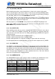
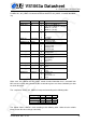
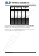
9 FUNCTIONAL DESCRIPTION
honouring DREQ. When SM_CANCEL is detected by a codec, it will stop decoding and return
to the main loop. The stream buffer content is discarded and the SM_CANCEL bit cleared.
SCI_HDAT1 will also be cleared. See Chapter 10.5.2 for details.
If SM_TESTS is set, SDI tests are allowed. For more details on SDI tests, look at Chapter 10.12.
SM_DACT defines the active edge of data clock for SDI. When ’0’, data is read at the rising
edge, when ’1’, data is read at the falling edge.
When SM_SDIORD is clear, bytes on SDI are sent MSb first. By setting SM_SDIORD, the user
may reverse the bit order for SDI, i.e. bit 0 is received first and bit 7 last. Bytes are, however,
still sent in the default order. This register bit has no effect on the SCI bus.
Setting SM_SDISHARE makes SCI and SDI share the same chip select, as explained in Chap-
ter 7.2, if also SM_SDINEW is set.
Setting SM_SDINEW will activate VS10xx native serial modes as described in Chapters 7.2.1 and 7.4.2.
Note, that this bit is set as a default when VS1063a is started up.
By activating SM_ENCODE and SM_RESET at the same time, the user will activate the en-
coding or codec mode (see Chapter 10.7 on page 55). However, note that if the recommended
VS1063a Patches package is used (http://www.vlsi.fi/en/support/software/vs10xxplugins.html),
then audio encoding is started as instructed in the manual of the package.
SM_LINE_IN is used to select the left-channel input for analog input. If ’0’, differential micro-
phone input pins MICP and MICN are used; if ’1’, line-level MICP/LINEIN1 pin is used.
SM_CLK_RANGE activates a clock divider in the XTAL input. When SM_CLK_RANGE is set,
the clock is divided by 2 at the input. From the chip’s point of view e.g. 24 MHz becomes
12 MHz. SM_CLK_RANGE should be set as soon as possible after a chip reset.
Version: 0.42, 2011-11-24 41