
Data Sheet


PRELIMINARY
VS1063a Datasheet
7 SPI BUSES
XCS up after sending the last bit of a data word, the next data word is sent immediately. After
the last data word, XCS is driven high as with a single word write.
After the last bit of a word has been sent, DREQ is driven low for the duration of the register
update, marked “execution” in the figure. The time varies depending on the register and its
contents (see table in Chapter 9.8 for details). If the maximum time is longer than what it takes
from the microcontroller to feed the next SCI command or SDI byte, status of DREQ must be
checked before finishing the next SCI/SDI operation.
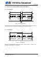
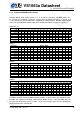
7.6 SPI Timing Diagram
XCS
SCK
SI
SO
0 1 1514 16
tXCSS
tXCSH
tWL tWH
tH
tSU
tV
tZ
tDIS
tXCS
30
31
Figure 9: SPI timing diagram
The SPI timing diagram is presented in Figure 9.
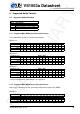
Symbol Min Max Unit
tXCSS 5 ns
tSU 0 ns
tH 2 CLKI cycles
tZ 0 ns
tWL 2 CLKI cycles
tWH 2 CLKI cycles
tV 2 (+ 25 ns
1
) CLKI cycles
tXCSH 1 CLKI cycles
tXCS 2 CLKI cycles
tDIS 10 ns
1
25 ns is when pin loaded with 100 pF capacitance. The time is shorter with lower capacitance.
Note: Although the timing is derived from the internal clock CLKI, the system always starts up in
1.0× mode, thus CLKI=XTALI. After you have configured a higher clock through SCI_CLOCKF
and waited for DREQ to rise, you can use a higher SPI speed as well.
Note: Because tWL + tWH + tH is 6×CLKI + 25 ns, the maximum speed for SCI reads is CLKI/7.
Version: 0.42, 2011-11-24 23