
Data Sheet


PRELIMINARY
VS1063a Datasheet
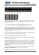
7 SPI BUSES
7.5.3 SCI Write
0 1 2 3 4 5 6 7 8 9 10 11 12 13 30 3114 15 16 17
0 0 0 0 0 0 1 0 0 0 0
3 2 1 0
1 0
X
address
XCS
SCK
SI
15 14
data out
0 0 0 0 0 0 0 0 0 0 0 0 0 0 0 0SO
0 0 0 0
X
0
instruction (write)
DREQ
execution
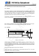
Figure 7: SCI word write
VS1063a registers are written from using the following sequence, as shown in Figure 7. First,
XCS line is pulled low to select the device. Then the WRITE opcode (0x2) is transmitted via the
SI line followed by an 8-bit word address.
After the word has been shifted in and the last clock has been sent, XCS should be pulled high
to end the WRITE sequence.
After the last bit has been sent, DREQ is driven low for the duration of the register update,
marked “execution” in the figure. The time varies depending on the register and its contents
(see table in Chapter 9.8 for details). If the maximum time is longer than what it takes from the
microcontroller to feed the next SCI command or SDI byte, status of DREQ must be checked
before finishing the next SCI/SDI operation.
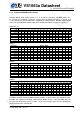
7.5.4 SCI Multiple Write
0 1 2 3 4 5 6 7 8 9 10 11 12 13 14 15 16 17
0 0 0 0 0 0 1 0 0 0 0
3 2 1 0
address
XCS
SCK
SI
15 14
0 0 0 0 0 0 0 0 0 0 0 0 0 0 0 0SO 0 0
0
instruction (write)
DREQ
1 0
X
0 0
X
execution
1
0 15 14
data out 1
data out 2
0 0 0 0
execution
X
31
30
32 3329
d.out n
m−2m−1
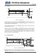
Figure 8: SCI multiple word write
VS1063a allows for the user to send multiple words to the same SCI register, which allows fast
SCI uploads, shown in Figure 8. The main difference to a single write is that instead of bringing
Version: 0.42, 2011-11-24 22