
Data Sheet
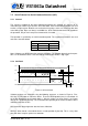


PRELIMINARY
VS1063a Datasheet
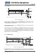
7 SPI BUSES
7.5 Serial Protocol for Serial Command Interface (SCI)
7.5.1 General
The serial bus protocol for the Serial Command Interface SCI (Chapter 9.7) consists of an
instruction byte, address byte and one 16-bit data word. Each read or write operation can read
or write a single register. Data bits are read at the rising edge, so the user should update data
at the falling edge. Bytes are always send MSb first. XCS should be low for the full duration of
the operation, but you can have pauses between bits if needed.
The operation is specified by an 8-bit instruction opcode. The supported instructions are read
and write. See table below.
Instruction
Name Opcode Operation
READ 0b0000 0011 Read data
WRITE 0b0000 0010 Write data
Note: VS1063a sets DREQ low after each SCI operation. The duration depends on the opera-
tion. It is not allowed to finish a new SCI/SDI operation before DREQ is high again.
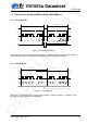
7.5.2 SCI Read
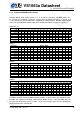
0 1 2 3 4 5 6 7 8 9 10 11 12 13 30 3114 15 16 17
0 0 0 0 0 0 1 1 0 0 0 0
3 2 1 0
0 0 0 0 0 0 0 0 0 0 0 0 0 0 0 0
15 14 1 0
X
instruction (read) address
data out
XCS
SCK
SI
SO
don’t care don’t care
DREQ
execution
Figure 6: SCI word read
VS1063a registers are read from using the following sequence, as shown in Figure 6. First,
XCS line is pulled low to select the device. Then the READ opcode (0x3) is transmitted via
the SI line followed by an 8-bit word address. After the address has been read in, any further
data on SI is ignored by the chip. The 16-bit data corresponding to the received address will be
shifted out onto the SO line.
XCS should be driven high after data has been shifted out.
DREQ is driven low for a short while when in a read operation by the chip. This is a very short
time and doesn’t require special user attention.
Version: 0.42, 2011-11-24 21