
Data Sheet


PRELIMINARY
VS1063a Datasheet
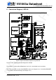
7 SPI BUSES
SDI Pin SCI Pin Description
- XCS Active low chip select input. A high level forces the serial interface into
standby mode, ending the current operation. A high level also forces serial
output (SO) to high impedance state.
BSYNC - SDI data is synchronized with a rising edge of BSYNC.
DCLK SCK Serial clock input. The serial clock is also used internally as the master
clock for the register interface.
SCK can be gated or continuous. In either case, the first rising clock edge
after XCS has gone low marks the first bit to be written.
SDATA SI Serial input. SI is sampled on the rising SCK edge, if XCS is low.
- SO Serial output. In reads, data is shifted out on the falling SCK edge.
In writes SO is at a high impedance state.
7.3 Data Request Pin DREQ
The DREQ pin/signal is used to signal if VS1063a’s 2048-byte FIFO is capable of receiving
data. If DREQ is high, VS1063a can take at least 32 bytes of SDI data or one SCI command.
DREQ is turned low when the stream buffer is too full and for the duration of a SCI command.
Because of the 32-byte safety area, the sender may send upto 32 bytes of SDI data at a
time without checking the status of DREQ, making controlling VS1063a easier for low-speed
microcontrollers.
Note: DREQ may turn low or high at any time, even during a byte transmission. Thus, DREQ
should only be used to decide whether to send more bytes. A transmission that has already
started doesn’t need to be aborted.
Note: In VS1063a DREQ also goes down while an SCI operation is in progress.
There are cases when you still want to send SCI commands when DREQ is low. Because
DREQ is shared between SDI and SCI, you can not determine if a SCI command has been
executed if SDI is not ready to receive. In this case you need a long enough delay after every
SCI command to make certain none of them is missed. The SCI Registers table in Chapter 9.8
gives the worst-case handling time for each SCI register write.
Version: 0.42, 2011-11-24 18