L7800 SERIES POSITIVE VOLTAGE REGULATORS ■ ■ ■ ■ ■ OUTPUT CURRENT TO 1.5A OUTPUT VOLTAGES OF 5; 5.2; 6; 8; 8.5; 9; 10; 12; 15; 18; 24V THERMAL OVERLOAD PROTECTION SHORT CIRCUIT PROTECTION OUTPUT TRANSITION SOA PROTECTION DESCRIPTION The L7800 series of three-terminal positive regulators is available in TO-220, TO-220FP, TO-220FM, TO-3 and D2PAK packages and several fixed output voltages, making it useful in a wide range of applications.
L7800 SERIES Table 1: Absolute Maximum Ratings Symbol VI Parameter DC Input Voltage Value for VO= 5 to 18V 35 for VO= 20, 24V 40 Unit V Output Current Internally Limited Ptot Power Dissipation Internally Limited Tstg Storage Temperature Range -65 to 150 °C Top Operating Junction Temperature for L7800 Range for L7800C -55 to 150 0 to 150 °C IO Absolute Maximum Ratings are those values beyond which damage to the device may occur. Functional operation under these condition is not implied.
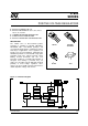
L7800 SERIES Figure 3: Connection Diagram (top view) TO-220 (Any Type) TO-220FP/TO-220FM D2PAK (Any Type) TO-3 Table 3: Order Codes TYPE L7805 L7805C L7852C L7806 L7806C L7808 L7808C L7885C L7809C L7810C L7812 L7812C L7815 L7815C L7818 L7818C L7820 L7820C L7824 L7824C TO-220 (A Type) TO-220 (C Type) L7805CV L7852CV TO-220 (E Type) D2PAK (A Type) (*) D2PAK (C Type) (T & R) TO-220FP TO-220FM L7805C-V L7805CV1 L7805CD2T L7805C-D2TR L7852CD2T L7805CP L7852CP L7805CF L7852CF L7806CV L7806C-V L
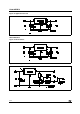
L7800 SERIES Figure 4: Application Circuits TEST CIRCUITS Figure 5: DC Parameter Figure 6: Load Regulation 4/34
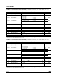
L7800 SERIES Figure 7: Ripple Rejection Table 4: Electrical Characteristics Of L7805 (refer to the test circuits, TJ = -55 to 150°C, VI = 10V, IO = 500 mA, CI = 0.33 µF, CO = 0.1 µF unless otherwise specified). Symbol Parameter Test Conditions Min. Typ. Max. VO Output Voltage TJ = 25°C VO Output Voltage IO = 5 mA to 1 A VI = 8 to 20 V ∆VO(*) Line Regulation VI = 7 to 25 V TJ = 25°C VI = 8 to 12 V TJ = 25°C IO = 5 mA to 1.
L7800 SERIES Table 5: Electrical Characteristics Of L7806 (refer to the test circuits, TJ = -55 to 150°C, VI = 11V, IO = 500 mA, CI = 0.33 µF, CO = 0.1 µF unless otherwise specified). Symbol Parameter Test Conditions VO Output Voltage TJ = 25°C VO Output Voltage IO = 5 mA to 1 A VI = 9 to 21 V ∆VO(*) Line Regulation VI = 8 to 25 V VI = 9 to 13 V ∆VO(*) Id ∆Id Load Regulation SVR Typ. Max. Unit 5.75 6 6.25 V 5.65 6 6.35 V TJ = 25°C 60 mV TJ = 25°C 30 IO = 5 mA to 1.
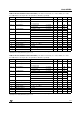
L7800 SERIES Table 7: Electrical Characteristics Of L7812 (refer to the test circuits, TJ = -55 to 150°C, VI = 19V, IO = 500 mA, CI = 0.33 µF, CO = 0.1 µF unless otherwise specified). Symbol Parameter Test Conditions VO Output Voltage TJ = 25°C VO Output Voltage IO = 5 mA to 1 A VI = 15.5 to 27 V ∆VO(*) Line Regulation VI = 14.5 to 30 V VI = 16 to 22 V ∆VO(*) Id ∆Id Load Regulation SVR Typ. Max. Unit 11.5 12 12.5 V 11.4 12 12.6 V TJ = 25°C 120 mV TJ = 25°C 60 IO = 5 mA to 1.
L7800 SERIES Table 9: Electrical Characteristics Of L7818 (refer to the test circuits, TJ = -55 to 150°C, VI = 26V, IO = 500 mA, CI = 0.33 µF, CO = 0.1 µF unless otherwise specified). Symbol Parameter Test Conditions VO Output Voltage TJ = 25°C VO Output Voltage IO = 5 mA to 1 A VI = 22 to 33 V ∆VO(*) Line Regulation VI = 21 to 33 V VI = 24 to 30 V ∆VO(*) Id ∆Id Load Regulation SVR Typ. Max. Unit 17.3 18 18.7 V 17.1 18 18.9 V TJ = 25°C 180 mV TJ = 25°C 90 IO = 5 mA to 1.
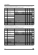
L7800 SERIES Table 11: Electrical Characteristics Of L7824 (refer to the test circuits, TJ = -55 to 150°C, VI = 33V, IO = 500 mA, CI = 0.33 µF, CO = 0.1 µF unless otherwise specified). Symbol Parameter Test Conditions Min. Typ. Max. VO Output Voltage TJ = 25°C VO Output Voltage IO = 5 mA to 1 A VI = 28 to 38 V ∆VO(*) Line Regulation VI = 27 to 38 V VI = 30 to 36 V IO = 5 mA to 1.5 A TJ = 25°C 240 IO = 250 to 750 mA TJ = 25°C 120 ∆VO(*) Id ∆Id Load Regulation SVR 23 24 25 V 22.
L7800 SERIES Table 13: Electrical Characteristics Of L7852C (refer to the test circuits, TJ = 0 to 125°C, VI = 10V, IO = 500 mA, CI = 0.33 µF, CO = 0.1 µF unless otherwise specified). Symbol Parameter Test Conditions Min. Typ. Max. VO Output Voltage TJ = 25°C VO Output Voltage IO = 5 mA to 1 A VI = 8 to 20 V ∆VO(*) Line Regulation VI = 7 to 25 V VI = 8 to 12 V IO = 5 mA to 1.5 A TJ = 25°C 105 IO = 250 to 750 mA TJ = 25°C 52 ∆VO(*) Id ∆Id Load Regulation SVR 5.0 5.2 5.4 V 4.95 5.
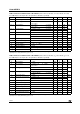
L7800 SERIES Table 15: Electrical Characteristics Of L7808C (refer to the test circuits, TJ = 0 to 125°C, VI = 14V, IO = 500 mA, CI = 0.33 µF, CO = 0.1 µF unless otherwise specified). Symbol Parameter Test Conditions VO Output Voltage TJ = 25°C VO Output Voltage IO = 5 mA to 1 A VI = 10.5 to 25 V ∆VO(*) Line Regulation VI = 10.5 to 25 V VI = 11 to 17 V ∆VO(*) Id ∆Id Load Regulation SVR Typ. Max. Unit 7.7 8 8.3 V 7.6 8 8.4 V TJ = 25°C 160 mV TJ = 25°C 80 IO = 5 mA to 1.
L7800 SERIES Table 17: Electrical Characteristics Of L7809C (refer to the test circuits, TJ = 0 to 125°C, VI = 15V, IO = 500 mA, CI = 0.33 µF, CO = 0.1 µF unless otherwise specified). Symbol Parameter Test Conditions Min. Typ. Max. VO Output Voltage TJ = 25°C VO Output Voltage IO = 5 mA to 1 A VI = 11.5 to 26 V ∆VO(*) Line Regulation VI = 11.5 to 26 V VI = 12 to 18 V IO = 5 mA to 1.5 A TJ = 25°C 180 IO = 250 to 750 mA TJ = 25°C 90 ∆VO(*) Id ∆Id Load Regulation SVR 8.64 9 9.36 V 8.
L7800 SERIES Table 19: Electrical Characteristics Of L7812C (refer to the test circuits, TJ = 0 to 125°C, VI = 19V, IO = 500 mA, CI = 0.33 µF, CO = 0.1 µF unless otherwise specified). Symbol Parameter Test Conditions Min. Typ. Max. VO Output Voltage TJ = 25°C VO Output Voltage IO = 5 mA to 1 A VI = 14.5 to 27 V ∆VO(*) Line Regulation VI = 14.5 to 30 V VI = 16 to 22 V IO = 5 mA to 1.5 A TJ = 25°C 240 IO = 250 to 750 mA TJ = 25°C 120 ∆VO(*) Id ∆Id Load Regulation SVR 11.5 12 12.
L7800 SERIES Table 21: Electrical Characteristics Of L7818C (refer to the test circuits, TJ = 0 to 125°C, VI = 26V, IO = 500 mA, CI = 0.33 µF, CO = 0.1 µF unless otherwise specified). Symbol Parameter Test Conditions Min. Typ. Max. VO Output Voltage TJ = 25°C VO Output Voltage IO = 5 mA to 1 A VI = 21 to 33 V ∆VO(*) Line Regulation VI = 21 to 33 V VI = 24 to 30 V IO = 5 mA to 1.
L7800 SERIES Table 23: Electrical Characteristics Of L7824C (refer to the test circuits, TJ = 0 to 125°C, VI = 33V, IO = 500 mA, CI = 0.33 µF, CO = 0.1 µF unless otherwise specified). Symbol Parameter Test Conditions Min. Typ. Max. VO Output Voltage TJ = 25°C VO Output Voltage IO = 5 mA to 1 A VI = 27 to 38 V ∆VO(*) Line Regulation VI = 27 to 38 V VI = 30 to 36 V IO = 5 mA to 1.
L7800 SERIES Figure 10: Supply Voltage Rejection vs Frequency Figure 13: Quiescent Current vs Junction Temperature Figure 11: Output Voltage vs Junction Temperature Figure 14: Load Transient Response Figure 12: Output Impedance vs Frequency Figure 15: Line Transient Response 16/34
L7800 SERIES Figure 16: Quiescent Current vs Input Voltage Figure 17: Fixed Output Regulator NOTE: 1. To specify an output voltage, substitute voltage value for "XX". 2. Although no output capacitor is need for stability, it does improve transient response. 3. Required if regulator is locate an appreciable distance from power supply filter.
L7800 SERIES Figure 19: Circuit for Increasing Output Voltage IR1 ≥ 5 Id R2 VO = VXX (1+ ) + Id R2 R1 Figure 20: Adjustable Output Regulator (7 to 30V) Figure 21: 0.
L7800 SERIES Figure 22: High Current Voltage Regulator VBEQ1 R1 = IQ1 IREQ - βQ1 VBEQ1 IO = IREG + Q1 (IREG ) R1 Figure 23: High Output Current with Short Circuit Protection VBEQ2 RSC = ISC Figure 24: Tracking Voltage Regulator 19/34
L7800 SERIES Figure 25: Split Power Supply (± 15V - 1 A) * Against potential latch-up problems.
L7800 SERIES Figure 28: High Input Voltage Circuit VIN = VI - (VZ + VBE) Figure 29: High Input Voltage Circuit Figure 30: High Output Voltage Regulator Figure 31: High Input and Output Voltage VO = VXX + VZ1 21/34
L7800 SERIES Figure 32: Reducing Power Dissipation with Dropping Resistor VI(min) - VXX - VDROP(max) R = IO(max) + Id(max) Figure 33: Remote Shutdown Figure 34: Power AM Modulator (unity voltage gain, IO ≤ 0.5) NOTE: The circuit performs well up to 100 KHz.
L7800 SERIES Figure 35: Adjustable Output Voltage with Temperature Compensation R2 VO = VXX (1+ ) + V BE R 1 NOTE: Q2 is connected as a diode in order to compensate the variation of the Q1 VBE with the temperature. C allows a slow rise time of the VO.
L7800 SERIES TO-3 MECHANICAL DATA mm. DIM. MIN. A inch TYP MAX. MIN. TYP. 11.85 B 0.96 MAX. 0.466 1.05 1.10 0.037 0.041 0.043 C 1.70 0.066 D 8.7 0.342 E 20.0 0.787 G 10.9 0.429 N 16.9 0.665 P 26.2 R 3.88 1.031 4.09 U 0.152 39.5 V 1.555 30.10 1.185 A P D C O N B V E G U 0.
L7800 SERIES TO-220 (A TYPE) MECHANICAL DATA DIM. mm. MIN. TYP inch MAX. MIN. A 4.40 4.60 0.173 TYP. MAX. 0.181 b 0.61 0.88 0.024 0.034 b1 1.15 1.70 0.045 0.067 c 0.49 0.70 0.019 0.027 D 15.25 15.75 0.600 0.620 E 10.0 10.40 0.393 0.409 e 2.4 2.7 0.094 0.106 e1 4.95 5.15 0.194 0.203 F 1.23 1.32 0.048 0.051 H1 6.2 6.6 0.244 0.260 J1 2.40 2.72 0.094 0.107 L 13.0 14.0 0.511 0.551 L1 3.5 3.93 0.137 0.154 L20 16.4 L30 0.645 28.9 1.
L7800 SERIES TO-220 (C TYPE) MECHANICAL DATA DIM. mm. MIN. MAX. MIN. A 4.30 4.70 0.169 0.185 b 0.70 0.90 0.028 0.035 b1 1.42 1.62 0.056 0.064 c 0.45 0.60 0.018 D E TYP inch 15.70 9.80 TYP. 0.024 0.618 10.20 0.386 0.402 e 2.54 0.100 e1 5.08 0.200 F 1.25 H1 MAX. 1.39 0.049 6.5 0.055 0.256 J1 2.20 2.60 0.087 0.202 L 12.88 13.28 0.507 0.523 L1 L20 3 15.70 L30 0.118 16.1 0.618 28.9 0.634 1.138 φP 3.50 3.70 0.138 0.146 Q 2.70 2.90 0.106 0.
L7800 SERIES TO-220 (E TYPE) MECHANICAL DATA DIM. mm. MIN. TYP inch MAX. MIN. A 4.47 4.67 0.176 TYP. 0.184 b 0.70 0.91 0.028 0.036 b1 1.17 1.37 0.046 0.054 c 0.31 0.53 0.012 0.021 D 14.60 15.70 0.575 0.618 E 9.96 10.36 0.392 0.408 e 2.54 0.100 e1 5.08 0.200 MAX. F 1.17 1.37 0.046 0.054 H1 6.1 6.8 0.240 0.268 J1 2.52 2.82 0.099 0.111 L 12.70 13.80 0.500 0.543 L1 3.20 3.96 0.126 0.156 L20 15.21 16.77 0.599 0.660 φP 3.73 3.94 0.
L7800 SERIES TO-220FP MECHANICAL DATA mm. DIM. MIN. TYP inch MAX. MIN. TYP. MAX. A 4.40 4.60 0.173 0.181 B 2.5 2.7 0.098 0.106 D 2.5 2.75 0.098 0.108 E 0.45 0.70 0.017 0.027 F 0.75 1 0.030 0.039 F1 1.15 1.50 0.045 0.059 F2 1.15 1.50 0.045 0.059 G 4.95 5.2 0.194 0.204 G1 2.4 2.7 0.094 0.106 H 10.0 10.40 0.393 L2 L3 16 0.409 0.630 28.6 30.6 1.126 1.204 L4 9.8 10.6 0.385 0.417 L5 2.9 3.6 0.114 0.142 L6 15.9 16.4 0.626 0.
L7800 SERIES TO-220FM MECHANICAL DATA DIM. mm. MIN. TYP inch MAX. MIN. TYP. MAX. A 4.50 4.90 0.177 0.193 B 2.34 2.74 0.092 0.108 D 2.56 2.96 0.101 0.117 E 0.45 0.60 0.018 F 0.70 0.90 0.028 0.50 F1 0.020 0.035 1.47 G 0.058 5.08 G1 2.34 H 9.96 L2 2.54 0.024 0.200 2.74 0.092 10.36 0.392 15.8 0.100 0.108 0.408 0.622 L4 9.45 10.05 0.372 0.396 L6 15.67 16.07 0.617 0.633 L7 8.99 9.39 0.354 0.370 L8 DIA. 3.30 3.08 0.130 3.28 0.121 0.
L7800 SERIES D2PAK (A TYPE) MECHANICAL DATA mm. inch DIM. MIN. TYP MAX. MIN. TYP. MAX. A 4.4 4.6 0.173 0.181 A1 0.03 0.23 0.001 0.009 b 0.7 0.93 0.027 0.036 b2 1.14 1.7 0.044 0.067 c 0.45 0.6 0.017 0.023 c2 1.23 1.36 0.048 0.053 D 8.95 8 9.35 0.352 0.368 E 10 10.4 E1 8.5 D1 e 0.315 0.393 0.409 0.335 2.54 0.100 e1 4.88 5.28 0.192 0.208 H 15 15.85 0.590 0.624 J1 2.49 2.69 0.098 0.106 L 2.29 2.79 0.090 0.110 L1 1.27 1.4 0.050 0.
L7800 SERIES D2PAK (C TYPE) MECHANICAL DATA mm. inch DIM. MIN. TYP MAX. MIN. TYP. MAX. A 4.3 4.7 0.169 0.185 A1 0 0.20 0.000 0.008 0.035 b 0.70 0.90 0.028 b2 1.17 1.37 0.046 c 0.45 0.50 0.6 0.018 0.020 0.024 c2 1.25 1.30 1.40 0.049 0.051 0.055 9.2 9.4 0.354 0.362 0.370 D 9.0 D1 7.5 E 9.8 E1 7.5 0.054 0.295 10.2 0.386 0.402 0.295 e 2.54 e1 5.08 0.200 H 15 J1 2.20 2.60 0.087 0.102 L 1.79 2.79 0.070 0.110 L1 1.0 1.4 0.039 0.
L7800 SERIES Tape & Reel D2PAK-P 2PAK-D 2PAK/A-P 2PAK/A MECHANICAL DATA mm. inch DIM. MIN. TYP A MIN. TYP. 180 13.0 13.2 MAX. 7.086 C 12.8 D 20.2 0.795 N 60 2.362 T 32/34 MAX. 0.504 0.512 14.4 0.519 0.567 Ao 10.50 10.6 10.70 0.413 0.417 0.421 Bo 15.70 15.80 15.90 0.618 0.622 0.626 Ko 4.80 4.90 5.00 0.189 0.193 0.197 Po 3.9 4.0 4.1 0.153 0.157 0.161 P 11.9 12.0 12.1 0.468 0.472 0.
L7800 SERIES Table 24: Revision History Date Revision 09-Nov-2004 12 Description of Changes Add New Part Number.
L7800 SERIES Information furnished is believed to be accurate and reliable. However, STMicroelectronics assumes no responsibility for the consequences of use of such information nor for any infringement of patents or other rights of third parties which may result from its use. No license is granted by implication or otherwise under any patent or patent rights of STMicroelectronics. Specifications mentioned in this publication are subject to change without notice.