
User Manual

MPU-9250 Register Map and Descriptions
Document Number: RM-MPU-9250A-00
Revision: 1.4
Release Date: 9/9/2013
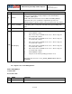
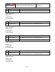
BIT
NAME
FUNCTION
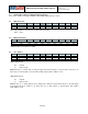
[4:0]
FIFO_CNT[12:8]
High Bits, count indicates the number of written bytes in the FIFO.
Reading this byte latches the data for both FIFO_COUNTH, and
FIFO_COUNTL.
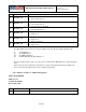
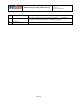
FIFO_COUNTL
Address: 115
Serial IF: Read Only
Reset value: 0x00
BIT
NAME
FUNCTION
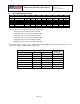
[7:0]
FIFO_CNT[7:0]
Low Bits, count indicates the number of written bytes in the
FIFO. NOTE: Must read FIFO_COUNTH to latch new data
for both FIFO_COUNTH and FIFO_COUNTL.
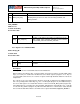
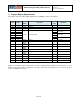
4.37 Register 116 – FIFO Read Write
Name: FIFO_R_W
Serial IF: R/W
Reset value: 0x00
BIT
NAME
FUNCTION
[7:0]
D[7:0]
Read/Write command provides Read or Write operation for
the FIFO.
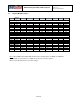
Description:
This register is used to read and write data from the FIFO buffer.
Data is written to the FIFO in order of register number (from lowest to highest). If all the FIFO enable
flags (see below) are enabled and all External Sensor Data registers (Registers 73 to 96) are
associated with a Slave device, the contents of registers 59 through 96 will be written in order at the
Sample Rate.
The contents of the sensor data registers (Registers 59 to 96) are written into the FIFO buffer when
their corresponding FIFO enable flags are set to 1 in FIFO_EN (Register 35). An additional flag for
the sensor data registers associated with I
2
C Slave 3 can be found in I2C_MST_CTRL (Register 36).
If the FIFO buffer has overflowed, the status bit FIFO_OFLOW_INT is automatically set to 1. This bit
is located in INT_STATUS (Register 58). When the FIFO buffer has overflowed, the oldest data will
be lost and new data will be written to the FIFO unless register 26 CONFIG, bit[6] FIFO_MODE = 1.
43 of 55