
User Manual


MPU-9250 Register Map and Descriptions
Document Number: RM-MPU-9250A-00
Revision: 1.4
Release Date: 9/9/2013
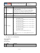
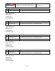
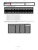
BIT
NAME
FUNCTION
[5]
CYCLE
When set, and SLEEP and STANDBY are not set, the chip will cycle
between sleep and taking a single sample at a rate determined by
LP_ACCEL_ODR register
NOTE: When all accelerometer axis are disabled via PWR_MGMT_2
register bits and cycle is enabled, the chip will wake up at the rate
determined by the respective registers above, but will not take any samples.
[4]
GYRO_STANDBY
When set, the gyro drive and pll circuitry are enabled, but the sense paths
are disabled. This is a low power mode that allows quick enabling of the
gyros.
[3]
PD_PTAT
Power down internal PTAT voltage generator and PTAT ADC
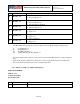
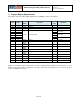
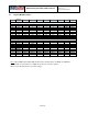
[2:0]
CLKSEL[2:0]
Code
Clock Source
0
Internal 20MHz oscillator
1
Auto selects the best available clock source – PLL if ready, else
use the Internal oscillator
2
Auto selects the best available clock source – PLL if ready, else
use the Internal oscillator
3
Auto selects the best available clock source – PLL if ready, else
use the Internal oscillator
4
Auto selects the best available clock source – PLL if ready, else
use the Internal oscillator
5
Auto selects the best available clock source – PLL if ready, else
use the Internal oscillator
6
Internal 20MHz oscillator
7
Stops the clock and keeps timing generator in reset
(After OTP loads, the inverse of PU_SLEEP_MODE bit will be written to
CLKSEL[0])
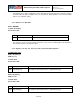
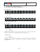
4.35 Register 108 – Power Management 2
Name: PWR_MGMT_2
Serial IF: R/W
Reset value: 0x00
BIT
NAME
FUNCTION
[7:6]
Reserved
41 of 55