
User Manual

MPU-9250 Register Map and Descriptions
Document Number: RM-MPU-9250A-00
Revision: 1.4
Release Date: 9/9/2013
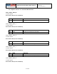
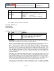
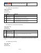
BIT
NAME
FUNCTION
[7]
Reserved
[6]
FIFO_EN
1 – Enable FIFO operation mode.
0 – Disable FIFO access from serial interface. To disable FIFO writes by
dma, use FIFO_EN register. To disable possible FIFO writes from DMP,
disable the DMP.
[5]
I2C_MST_EN
1 – Enable the I2C Master I/F module; pins ES_DA and ES_SCL are isolated
from pins SDA/SDI and SCL/ SCLK.
0 – Disable I2C Master I/F module; pins ES_DA and ES_SCL are logically
driven by pins SDA/SDI and SCL/ SCLK.
NOTE: DMP will run when enabled, even if all internal sensors are disabled,
except when the sample rate is set to 8Khz.
[4]
I2C_IF_DIS
1 – Reset I2C Slave module and put the serial interface in SPI mode only.
This bit auto clears after one clock cycle.
[3]
Reserved
[2]
FIFO_RST
1 – Reset FIFO module. Reset is asynchronous. This bit auto clears after
one clock cycle.
[1]
I2C_MST_RST
1 – Reset I2C Master module. Reset is asynchronous. This bit auto clears
after one clock cycle.
NOTE: This bit should only be set when the I2C master has hung. If this bit
is set during an active I2C master transaction, the I2C slave will hang, which
will require the host to reset the slave.
[0]
SIG_COND_RST
1 – Reset all gyro digital signal path, accel digital signal path, and temp
digital signal path. This bit also clears all the sensor registers.
SIG_COND_RST is a pulse of one clk8M wide.
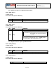
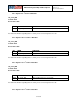
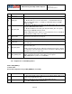
4.34 Register 107 – Power Management 1
Name: PWR_MGMT_1
Serial IF: R/W
Reset value: (Depends on PU_SLEEP_MODE bit, see below)
BIT
NAME
FUNCTION
[7]
H_RESET
1 – Reset the internal registers and restores the default settings. Write a 1 to
set the reset, the bit will auto clear.
[6]
SLEEP
When set, the chip is set to sleep mode (After OTP loads, the
PU_SLEEP_MODE bit will be written here)
40 of 55