
User Manual

MPU-9250 Register Map and Descriptions
Document Number: RM-MPU-9250A-00
Revision: 1.4
Release Date: 9/9/2013
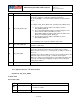
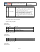
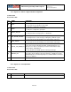
4.19 Register 55 – INT Pin / Bypass Enable Configuration
Serial IF: R/W
Reset value: 0x00
BIT
NAME
FUNCTION
[7]
ACTL
1 – The logic level for INT pin is active low.
0 – The logic level for INT pin is active high.
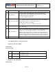
[6]
OPEN
1 – INT pin is configured as open drain.
0 – INT pin is configured as push-pull.
[5]
LATCH_INT_EN
1 – INT pin level held until interrupt status is cleared.
0 – INT pin indicates interrupt pulse’s is width 50us.
[4]
INT_ANYRD_2CLEAR
1 – Interrupt status is cleared if any read operation is performed.
0 – Interrupt status is cleared only by reading INT_STATUS register
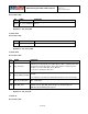
[3]
ACTL_FSYNC
1 – The logic level for the FSYNC pin as an interrupt is active low.
0 – The logic level for the FSYNC pin as an interrupt is active high.
[2]
FSYNC_INT_MODE_EN
1 – This enables the FSYNC pin to be used as an interrupt. A transition
to the active level described by the ACTL_FSYNC bit will cause an
interrupt. The status of the interrupt is read in the I2C Master Status
register PASS_THROUGH bit.
0 – This disables the FSYNC pin from causing an interrupt.
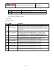
[1]
BYPASS_EN
When asserted, the i2c_master interface pins(ES_CL and ES_DA) will go
into ‘bypass mode’ when the i2c master interface is disabled. The pins
will float high due to the internal pull-up if not enabled and the i2c master
interface is disabled.
[0]
RESERVED
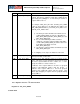
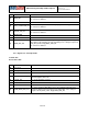
4.20 Register 56 – Interrupt Enable
Serial IF: R/W
Reset value: 0x00
BIT
NAME
FUNCTION
[7]
RESERVED
29 of 55