
User Manual

MPU-9250 Register Map and Descriptions
Document Number: RM-MPU-9250A-00
Revision: 1.4
Release Date: 9/9/2013
Reset value: 0x00
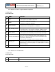
BIT
NAME
FUNCTION
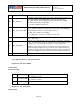
[7]
I2C_SLV2_RNW
1 – Transfer is a read
0 – Transfer is a write
[6:0]
I2C_ID_2[6:0]
Physical address of I2C slave 2
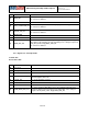
Register 44 - I2C_SLV2_REG
Serial IF: R/W
Reset value: 0x00
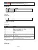
BIT
NAME
FUNCTION
[7:0]
I2C_SLV2_REG[7:0]
I2C slave 2 register address from where to begin data
transfer
Register 45 - I2C_SLV2_CTRL
Serial IF: R/W
Reset value: 0x00
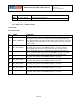
BIT
NAME
FUNCTION
[7]
I2C_SLV2_EN
1 – Enable reading data from this slave at the sample rate
and storing data at the first available EXT_SENS_DATA
register as determined by I2C_SLV0_EN, I2C_SLV0_LENG,
I2C_SLV1_EN and I2C_SLV1_LENG.
0 – function is disabled for this slave
[6]
I2C_SLV2_BYTE_SW
1 – Swap bytes when reading both the low and high byte of
a word. Note there is nothing to swap after reading the first
byte if I2C_SLV2_REG[0] = 1, or if the last byte read has a
register address lsb = 0.
See I2C_SLV1_CTRL for an example.
0 – no swapping occurs, bytes are written in order read.
[5]
I2C_SLV2_REG_DIS
When set, the transaction does not write a register value, it
will only read data, or write data
24 of 55