
User Manual

MPU-9250 Register Map and Descriptions
Document Number: RM-MPU-9250A-00
Revision: 1.4
Release Date: 9/9/2013
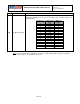
4.13 Registers 37 to 39 – I
2
C Slave 0 Control
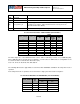
Register 37 - I2C_SLV0_ADDR
Serial IF: R/W
Reset value: 0x00
BIT
NAME
FUNCTION
[7]
I2C_SLV0_RNW
1 – Transfer is a read
0 – Transfer is a write
[6:0]
I2C_ID_0[6:0]
Physical address of I2C slave 0
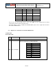
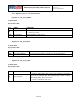
Register 38 - I2C_SLV0_REG
Serial IF: R/W
Reset value: 0x00
BIT
NAME
FUNCTION
[7:0]
I2C_SLV0_REG[7:0]
I2C slave 0 register address from where to begin data transfer
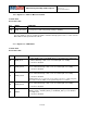
Register 39 - I2C_SLV0_CTRL
Serial IF: R/W
Reset value: 0x00
BIT
NAME
FUNCTION
[7]
I2C_SLV0_EN
1 – Enable reading data from this slave at the sample rate and storing
data at the first available EXT_SENS_DATA register, which is always
EXT_SENS_DATA_00 for I2C slave 0.
0 – function is disabled for this slave
20 of 55