InvenSense Inc. 1745 Technology Drive, San Jose, CA 95110 U.S.A. Tel: +1 (408) 988-7339 Fax: +1 (408) 988-8104 Website: www.invensense.com Document Number: RM-MPU-9250A-00 Revision: 1.4 Release Date: 9/9/2013 MPU-9250 Register Map and Descriptions Revision 1.
MPU-9250 Register Map and Descriptions Document Number: RM-MPU-9250A-00 Revision: 1.4 Release Date: 9/9/2013 CONTENTS 1 REVISION HISTORY ................................................................................................................................... 5 2 PURPOSE AND SCOPE ............................................................................................................................. 6 3 REGISTER MAP FOR GYROSCOPE AND ACCELEROMETER .......................................
MPU-9250 Register Map and Descriptions Document Number: RM-MPU-9250A-00 Revision: 1.4 Release Date: 9/9/2013 REGISTER 49 - I2C_SLV4_ADDR ..................................................................................................................26 REGISTER 50 - I2C_SLV4_REG ....................................................................................................................26 REGISTER 51 - I2C_SLV4_DO ....................................................................................
MPU-9250 Register Map and Descriptions 6 Document Number: RM-MPU-9250A-00 Revision: 1.4 Release Date: 9/9/2013 5.7 ST2: STATUS 2 .................................................................................................................................51 5.8 CNTL1: CONTROL 1 ..........................................................................................................................51 5.9 CNTL2: CONTROL 2 ............................................................................
MPU-9250 Register Map and Descriptions 1 Revision History Revision Date Revision Description 9/9/2013 1.4 Initial release 5 of 55 Document Number: RM-MPU-9250A-00 Revision: 1.
MPU-9250 Register Map and Descriptions 2 Document Number: RM-MPU-9250A-00 Revision: 1.4 Release Date: 9/9/2013 Purpose and Scope This document provides preliminary information regarding the register map and descriptions for the Motion Processing Unit™ MPU-9250™. This document should be used in conjunction with the MPU-9250 Product Specification (PS-MPU-9250A-00) for detailed features, specifications, and other product information.
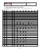
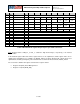
Document Number: RM-MPU-9250A-00 Revision: 1.4 Release Date: 9/9/2013 MPU-9250 Register Map and Descriptions 3 Register Map for Gyroscope and Accelerometer The following table lists the register map for the gyroscope and accelerometer in the MPU-9250 MotionTracking device. Addr (Hex) Addr (Dec.
MPU-9250 Register Map and Descriptions Addr (Hex) Addr (Dec.) 35 53 Register Name I2C_SLV4_DI Serial I/F Bit7 Bit6 Bit5 Bit4 R PASS_ THROUGH I2C_SLV4 _DONE I2C_LOST _ARB I2C_SLV4 _NACK R Document Number: RM-MPU-9250A-00 Revision: 1.
Document Number: RM-MPU-9250A-00 Revision: 1.4 Release Date: 9/9/2013 MPU-9250 Register Map and Descriptions Addr (Hex) Addr (Dec.
MPU-9250 Register Map and Descriptions 4 Document Number: RM-MPU-9250A-00 Revision: 1.4 Release Date: 9/9/2013 Register Descriptions This section describes the function and contents of each register within the MPU-9250. All the descriptions relate to the default MPU-9250 mode of operation. 4.
MPU-9250 Register Map and Descriptions 4.3 Document Number: RM-MPU-9250A-00 Revision: 1.4 Release Date: 9/9/2013 Registers 19 to 24 – Gyro Offset Registers Serial IF: R/W Reset value: 0x00 BIT NAME FUNCTION High byte, Low byte in USR register (14h) [7:0] [7:0] X_OFFS_USR[15:8] X_OFFS_USR[7:0] OffsetLSB= X_OFFS_USR * 4 / 2^FS_SEL OffsetDPS= X_OFFS_USR * 4 / 2^FS_SEL / Gyro_Sensitivity Nominal FS_SEL = 0 Conditions Gyro_Sensitivity = 2^16 LSB / 500dps Max 999.
MPU-9250 Register Map and Descriptions Document Number: RM-MPU-9250A-00 Revision: 1.4 Release Date: 9/9/2013 These registers are used to remove DC bias from the gyro sensor data output for X, Y and Z axes. The values in these registers are subtracted from the gyro sensor values before going into the sensor registers. Please refer to registers 67 to 72 for units. 4.
MPU-9250 Register Map and Descriptions [5:3] EXT_SYNC_SET[2:0] Document Number: RM-MPU-9250A-00 Revision: 1.4 Release Date: 9/9/2013 Enables the FSYNC pin data to be sampled. EXT_SYNC_SET FSYNC bit location 0 function disabled 1 TEMP_OUT_L[0] 2 GYRO_XOUT_L[0] 3 GYRO_YOUT_L[0] 4 GYRO_ZOUT_L[0] 5 ACCEL_XOUT_L[0] 6 ACCEL_YOUT_L[0] 7 ACCEL_ZOUT_L[0] Fsync will be latched to capture short strobes.
MPU-9250 Register Map and Descriptions Document Number: RM-MPU-9250A-00 Revision: 1.4 Release Date: 9/9/2013 Serial IF: R/W Reset value: 0x00 BIT NAME FUNCTION [7] XGYRO_Cten X Gyro self-test [6] YGYRO_Cten Y Gyro self-test [5] ZGYRO_Cten Z Gyro self-test Gyro Full Scale Select: 00 = +250dps [4:3] GYRO_FS_SEL[1:0] 01= +500 dps 10 = +1000 dps 11 = +2000 dps [2] - Reserved [1:0] Fchoice_b[1:0] Used to bypass DLPF as shown in table 1 above.
Document Number: RM-MPU-9250A-00 Revision: 1.4 Release Date: 9/9/2013 MPU-9250 Register Map and Descriptions BIT NAME FUNCTION [7:6] Reserved [5:4] Reserved [3] accel_fchoice_b Used to bypass DLPF as shown in table 2 below. NOTE: This register contains accel_fchoice_b (the inverted version of accel_fchoice as described in the table below). [2:0] A_DLPFCFG Accelerometer low pass filter setting as shown in table 2 below.
MPU-9250 Register Map and Descriptions Document Number: RM-MPU-9250A-00 Revision: 1.4 Release Date: 9/9/2013 0 3.91 1.1 k 1 0 7.81 1.1 k 1 0 15.63 1.1 k 1 0 31.25 1.1 k 1 0 62.50 1.1 k 1 0 125 1.1 k 1 0 250 1.1 k 1 0 500 1.1 kHz 1 As you can see from the tables above, some of the ODRs can be configured in the normal accelerometer mode as well as low power mode.
MPU-9250 Register Map and Descriptions Document Number: RM-MPU-9250A-00 Revision: 1.4 Release Date: 9/9/2013 4.10 Register 31 – Wake-on Motion Threshold Serial IF: R/W Reset value: 0x00 BIT NAME FUNCTION [7:0] WOM_Threshold This register holds the threshold value for the Wake on Motion Interrupt for accel x/y/z axes. LSB = 4mg. Range is 0mg to 1020mg. For more details on how to configure the Wake-on-Motion interrupt, please refer to section 5 in the MPU-9250 Product Specification document. 4.
MPU-9250 Register Map and Descriptions BIT [2] Document Number: RM-MPU-9250A-00 Revision: 1.
MPU-9250 Register Map and Descriptions BIT NAME Document Number: RM-MPU-9250A-00 Revision: 1.4 Release Date: 9/9/2013 FUNCTION I2C_MST_CLK is a 4 bit unsigned value which configures a divider on the MPU2 9250 internal 8MHz clock.
MPU-9250 Register Map and Descriptions Document Number: RM-MPU-9250A-00 Revision: 1.4 Release Date: 9/9/2013 2 4.
MPU-9250 Register Map and Descriptions BIT NAME Document Number: RM-MPU-9250A-00 Revision: 1.4 Release Date: 9/9/2013 FUNCTION 1 – Swap bytes when reading both the low and high byte of a word. Note there is nothing to swap after reading the first byte if I2C_SLV0_REG[0] = 1, or if the last byte read has a register address lsb = 0.
MPU-9250 Register Map and Descriptions Document Number: RM-MPU-9250A-00 Revision: 1.
MPU-9250 Register Map and Descriptions BIT NAME [6] I2C_SLV1_BYTE_SW Document Number: RM-MPU-9250A-00 Revision: 1.4 Release Date: 9/9/2013 FUNCTION 1 – Swap bytes when reading both the low and high byte of a word. Note there is nothing to swap after reading the first byte if I2C_SLV1_REG[0] = 1, or if the last byte read has a register address lsb = 0.
MPU-9250 Register Map and Descriptions Document Number: RM-MPU-9250A-00 Revision: 1.
MPU-9250 Register Map and Descriptions BIT NAME Document Number: RM-MPU-9250A-00 Revision: 1.4 Release Date: 9/9/2013 FUNCTION External sensor data typically comes in as groups of two bytes. This bit is used to determine if the groups are from the slave’s register address 0 and 1, 2 and 3, etc.., or if the groups are address 1 and 2, 3 and 4, etc.. [4] I2C_SLV2_GRP 0 indicates slave register addresses 0 and 1 are grouped together (odd numbered register ends the group).
MPU-9250 Register Map and Descriptions BIT [7] NAME Document Number: RM-MPU-9250A-00 Revision: 1.4 Release Date: 9/9/2013 FUNCTION I2C_SLV3_EN 1 – Enable reading data from this slave at the sample rate and storing data at the first available EXT_SENS_DATA register as determined by I2C_SLV0_EN, I2C_SLV0_LENG, I2C_SLV1_EN, I2C_SLV1_LENG, I2C_SLV2_EN and I2C_SLV2_LENG. 0 – function is disabled for this slave [6] I2C_SLV3_BYTE_SW 1 – Swap bytes when reading both the low and high byte of a word.
MPU-9250 Register Map and Descriptions Document Number: RM-MPU-9250A-00 Revision: 1.4 Release Date: 9/9/2013 Reset value: 0x00 BIT NAME FUNCTION [7:0] I2C_SLV4_REG[7:0] I2C slave 4 register address from where to begin data transfer Register 51 - I2C_SLV4_DO Serial IF: R/W Reset value: 0x00 BIT NAME FUNCTION [7:0] I2C_SLV4_DO[7:0] Data to be written to I2C Slave 4 if enabled.
MPU-9250 Register Map and Descriptions BIT NAME FUNCTION [7:0] I2C_SLV4_DI[7:0] Data read from I2C Slave 4. Document Number: RM-MPU-9250A-00 Revision: 1.4 Release Date: 9/9/2013 2 4.18 Register 54 – I C Master Status Serial IF: R/C Reset value: 0x00 BIT NAME FUNCTION [7] PASS_THROUGH Status of FSYNC interrupt – used as a way to pass an external interrupt through this chip to the host.
MPU-9250 Register Map and Descriptions Document Number: RM-MPU-9250A-00 Revision: 1.4 Release Date: 9/9/2013 4.19 Register 55 – INT Pin / Bypass Enable Configuration Serial IF: R/W Reset value: 0x00 BIT NAME [7] ACTL [6] OPEN [5] LATCH_INT_EN [4] INT_ANYRD_2CLEAR [3] ACTL_FSYNC [2] FSYNC_INT_MODE_EN FUNCTION 1 – The logic level for INT pin is active low. 0 – The logic level for INT pin is active high. 1 – INT pin is configured as open drain. 0 – INT pin is configured as push-pull.
MPU-9250 Register Map and Descriptions BIT NAME [6] WOM_EN [5] RESERVED [4] FIFO_OVERFLOW_EN [3] FSYNC_INT_EN [2] RESERVED [1] RESERVED [0] RAW_RDY_EN Document Number: RM-MPU-9250A-00 Revision: 1.4 Release Date: 9/9/2013 FUNCTION 1 – Enable interrupt for wake on motion to propagate to interrupt pin. 0 – function is disabled. 1 – Enable interrupt for fifo overflow to propagate to interrupt pin. 0 – function is disabled. 1 – Enable Fsync interrupt to propagate to interrupt pin.
MPU-9250 Register Map and Descriptions Document Number: RM-MPU-9250A-00 Revision: 1.4 Release Date: 9/9/2013 4.22 Registers 59 to 64 – Accelerometer Measurements Name: ACCEL_XOUT_H Serial IF: SyncR Reset value: 0x00 (if sensor disabled) BIT NAME FUNCTION [7:0] D[7:0] High byte of accelerometer x-axis data. Name: ACCEL_XOUT_L Serial IF: SyncR Reset value: 0x00 (if sensor disabled) BIT NAME FUNCTION [7:0] D[7:0] Low byte of accelerometer x-axis data.
MPU-9250 Register Map and Descriptions Document Number: RM-MPU-9250A-00 Revision: 1.4 Release Date: 9/9/2013 BIT NAME FUNCTION [7:0] D[7:0] High byte of accelerometer z-axis data. Name: ACCEL_ZOUT_L Serial IF: SyncR Reset value: 0x00 (if sensor disabled) BIT NAME FUNCTION [7:0] D[7:0] Low byte of accelerometer z-axis data.
MPU-9250 Register Map and Descriptions Document Number: RM-MPU-9250A-00 Revision: 1.4 Release Date: 9/9/2013 4.
MPU-9250 Register Map and Descriptions BIT NAME Document Number: RM-MPU-9250A-00 Revision: 1.
MPU-9250 Register Map and Descriptions BIT NAME Document Number: RM-MPU-9250A-00 Revision: 1.4 Release Date: 9/9/2013 FUNCTION Low byte of the Z-Axis gyroscope output [7:0] D[7:0] GYRO_ZOUT = Gyro_Sensitivity * Z_angular_rate Nominal FS_SEL = 0 Conditions Gyro_Sensitivity = 131 LSB/(º/s) 4.
MPU-9250 Register Map and Descriptions Document Number: RM-MPU-9250A-00 Revision: 1.4 Release Date: 9/9/2013 registers and hence the total read lengths between all the slaves cannot be greater than 24 or some bytes will be lost. Note: Slave 4’s behavior is distinct from that of Slaves 0-3. For further information regarding the characteristics of Slave 4, please refer to Registers 49 to 53.
MPU-9250 Register Map and Descriptions Document Number: RM-MPU-9250A-00 Revision: 1.4 Release Date: 9/9/2013 2 4.26 Register 99 – I C Slave 0 Data Out I2C_SLV0_DO Serial IF: R/W Reset value: 0x00 BIT NAME FUNCTION [7:0] I2C_SLV0_DO Data out when slave 0 is set to write For further information regarding Slave 1 control, please refer to Registers 37 to 39. 2 4.
MPU-9250 Register Map and Descriptions Document Number: RM-MPU-9250A-00 Revision: 1.4 Release Date: 9/9/2013 I2C_SLV3_DO Serial IF: R/W Reset value: 0x00 BIT NAME FUNCTION [7:0] I2C_SLV3_DO Data out when slave 3 is set to write For further information regarding Slave 2 control, please refer to Registers 46 to 48. 2 4.
MPU-9250 Register Map and Descriptions Document Number: RM-MPU-9250A-00 Revision: 1.4 Release Date: 9/9/2013 4.31 Register 104 – Signal Path Reset SIGNAL_PATH_RESET Serial IF: R/W Reset value: 0x00 BIT NAME FUNCTION [7:3] Reserved [2] GYRO_RST Reset gyro digital signal path. Note: Sensor registers are not cleared. Use SIG_COND_RST to clear sensor registers. [1] ACCEL_RST Reset accel digital signal path. Note: Sensor registers are not cleared. Use SIG_COND_RST to clear sensor registers.
MPU-9250 Register Map and Descriptions BIT NAME [7] Reserved Document Number: RM-MPU-9250A-00 Revision: 1.4 Release Date: 9/9/2013 FUNCTION 1 – Enable FIFO operation mode. [6] FIFO_EN 0 – Disable FIFO access from serial interface. To disable FIFO writes by dma, use FIFO_EN register. To disable possible FIFO writes from DMP, disable the DMP. 1 – Enable the I2C Master I/F module; pins ES_DA and ES_SCL are isolated from pins SDA/SDI and SCL/ SCLK.
MPU-9250 Register Map and Descriptions BIT NAME Document Number: RM-MPU-9250A-00 Revision: 1.4 Release Date: 9/9/2013 FUNCTION When set, and SLEEP and STANDBY are not set, the chip will cycle between sleep and taking a single sample at a rate determined by LP_ACCEL_ODR register [5] CYCLE [4] GYRO_STANDBY When set, the gyro drive and pll circuitry are enabled, but the sense paths are disabled. This is a low power mode that allows quick enabling of the gyros.
MPU-9250 Register Map and Descriptions BIT NAME [5] DISABLE_XA [4] DISABLE_YA [3] DISABLE_ZA [2] DISABLE_XG [1] DISABLE_YG [0] DISABLE_ZG Document Number: RM-MPU-9250A-00 Revision: 1.
MPU-9250 Register Map and Descriptions BIT NAME Document Number: RM-MPU-9250A-00 Revision: 1.4 Release Date: 9/9/2013 FUNCTION High Bits, count indicates the number of written bytes in the FIFO. [4:0] FIFO_CNT[12:8] Reading this byte latches the data for both FIFO_COUNTH, and FIFO_COUNTL. FIFO_COUNTL Address: 115 Serial IF: Read Only Reset value: 0x00 BIT NAME FUNCTION [7:0] FIFO_CNT[7:0] Low Bits, count indicates the number of written bytes in the FIFO.
MPU-9250 Register Map and Descriptions Document Number: RM-MPU-9250A-00 Revision: 1.4 Release Date: 9/9/2013 If the FIFO buffer is empty, reading this register will return the last byte that was previously read from the FIFO until new data is available. The user should check FIFO_COUNT to ensure that the FIFO buffer is not read when empty. 4.
MPU-9250 Register Map and Descriptions BIT NAME [0] Reserved Document Number: RM-MPU-9250A-00 Revision: 1.4 Release Date: 9/9/2013 FUNCTION Name: YA_OFFS_H Address: 122 Serial IF: R/W Reset value: 0x00 BIT NAME FUNCTION [7:0] YA_OFFS[14:7] Upper bits of the Y accelerometer offset cancellation. +/- 16g Offset cancellation in all Full Scale modes, 15 bit 0.
MPU-9250 Register Map and Descriptions Document Number: RM-MPU-9250A-00 Revision: 1.4 Release Date: 9/9/2013 BIT NAME FUNCTION [7:1] ZA_OFFS[6:0] Lower bits of the Z accelerometer offset cancellation. +/- 16g Offset cancellation in all Full Scale modes, 15 bit 0.
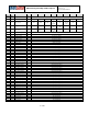
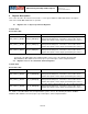
MPU-9250 Register Map and Descriptions 5 Document Number: RM-MPU-9250A-00 Revision: 1.4 Release Date: 9/9/2013 Register Map for Magnetometer The register map for the MPU-9250’s Magnetometer (AK8963) section is listed below.
MPU-9250 Register Map and Descriptions 5.1 Document Number: RM-MPU-9250A-00 Revision: 1.
MPU-9250 Register Map and Descriptions Document Number: RM-MPU-9250A-00 Revision: 1.4 Release Date: 9/9/2013 5.2 Detailed Descriptions for Magnetometer Registers This section details each register within the MPU-9250’s Magnetometer section. 5.3 WIA: Device ID Addr Register name D7 D6 D5 D4 D3 D2 D1 D0 0 1 0 0 0 D4 D3 D2 D1 D0 INFO5 INFO4 INFO3 INFO2 INFO1 INFO0 D5 D4 D3 D2 D1 D0 0 0 0 0 0 0 0 0 DRDY 0 Read-only register 00H WIA 0 1 0 Device ID of AKM.
MPU-9250 Register Map and Descriptions 5.6 Document Number: RM-MPU-9250A-00 Revision: 1.
MPU-9250 Register Map and Descriptions 5.7 Document Number: RM-MPU-9250A-00 Revision: 1.
Document Number: RM-MPU-9250A-00 Revision: 1.4 Release Date: 9/9/2013 MPU-9250 Register Map and Descriptions When each mode is set, AK8963 transits to set mode. When CNTL register is accessed to be written, registers from 02H to 09H are initialized. 5.9 CNTL2: Control 2 Addr Register name D7 D6 D5 D4 D3 CNTL2 0 0 0 0 0 0 0 0 0 0 D2 D1 D0 0 0 SRST 0 0 0 Read-only register 0BH Reset SRST: Soft reset "0": Normal "1": Reset When “1” is set, all registers are initialized.
MPU-9250 Register Map and Descriptions 2 Document Number: RM-MPU-9250A-00 Revision: 1.4 Release Date: 9/9/2013 2 2 This register disables I C bus interface. I C bus interface is enabled in default. To disable I C bus 2 interface, write “00011011” to I2CDIS register. Then I C bus interface is disabled. 2 Once I C bus interface is disabled, it is impossible to write other value to I2CDIS register. To enable I2C bus interface, reset AK8963 or input start condition 8 times continuously. 5.
MPU-9250 Register Map and Descriptions 6 Document Number: RM-MPU-9250A-00 Revision: 1.4 Release Date: 9/9/2013 Advanced Hardware Features The MPU-9250 includes advanced hardware features that support Android that can be enabled and disabled through simple hardware register settings. The advanced hardware features are not initially enabled after device power up, and must be individually enabled and configured.
MPU-9250 Register Map and Descriptions Document Number: RM-MPU-9250A-00 Revision: 1.4 Release Date: 9/9/2013 This information furnished by InvenSense is believed to be accurate and reliable. However, no responsibility is assumed by InvenSense for its use, or for any infringements of patents or other rights of third parties that may result from its use. Specifications are subject to change without notice.