
Data Sheet

MPU-9250 Product Specification
Document Number: PS-MPU-9250A-01
Revision: 1.0
Release Date: 01/17/2014
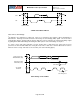
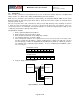
To read the internal MPU-9250 registers, the master sends a start condition, followed by the I
2
C address and
a write bit, and then the register address that is going to be read. Upon receiving the ACK signal from the
MPU-9250, the master transmits a start signal followed by the slave address and read bit. As a result, the
MPU-9250 sends an ACK signal and the data. The communication ends with a not acknowledge (NACK)
signal and a stop bit from master. The NACK condition is defined such that the SDA line remains high at the
9
th
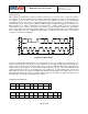
clock cycle. The following figures show single and two-byte read sequences.
Single-Byte Read Sequence
Burst Read Sequence
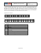
7.4 I2C Terms
Signal
Description
S
Start Condition: SDA goes from high to low while SCL is high
AD
Slave I
2
C address
W
Write bit (0)
R
Read bit (1)
ACK
Acknowledge: SDA line is low while the SCL line is high at the
9
th
clock cycle
NACK
Not-Acknowledge: SDA line stays high at the 9
th
clock cycle
RA
MPU-9250 internal register address
DATA
Transmit or received data
P
Stop condition: SDA going from low to high while SCL is high
Master
S
AD+W
RA
S
AD+R
NACK
P
Slave
ACK
ACK
ACK
DATA
Master
S
AD+W
RA
S
AD+R
ACK
NACK
P
Slave
ACK
ACK
ACK
DATA
DATA
Page 35 of 42