
Data Sheet

MPU-9250 Product Specification
Document Number: PS-MPU-9250A-01
Revision: 1.0
Release Date: 01/17/2014
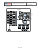
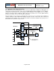
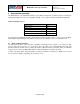
4.14 MPU-9250 Solution Using SPI Interface
In the figure below, the system processor is a SPI master to the MPU-9250. The CS, SDO, SCLK, and SDI
signals are used for SPI communications. Because these SPI pins are shared with the I
2
C slave pins, the
system processor cannot access the auxiliary I
2
C bus through the interface bypass multiplexer, whic h
connects the processor I
2
C interface pins to the sensor I
2
C interface pins.
Since the MPU-9250 has limited capabilities as an I
2
C Master, and depends on the system processor to
manage the initial configuration of any auxiliary sensors, another method must be used for programming the
sensors on the auxiliary sensor I
2
C bus (AUX_DA and AUX_CL).
When using SPI communications between the MPU-9250 and the system processor, configuration of
devices on the auxiliary I
2
C sensor bus can be achieved by using I
2
C Slaves 0-4 to perform read and write
transactions on any device and register on the auxiliary I
2
C bus. The I
2
C Slave 4 interface can be used to
perform only single byte read and write transactions.
Once the external sensors have been configured, the MPU-9250 can perform single or multi-byte reads
using the sensor I
2
C bus. The read results from the Slave 0-3 controllers can be written to the FIFO buffer as
well as to the external sensor registers.
The INT pin should be connected to a GPIO on the system processor capable of waking the processor from
suspend
For further information regarding the control of the MPU-9250’s auxiliary I
2
C interface, please refer to the
MPU-9250 Register Map and Register Descriptions document.
MPU-9250
SDO
SCLK
SDI
Digital
Motion
Processor
(DMP)
Sensor
Master I
2
C
Serial
Interface
Interrupt
Status
Register
INT
FIFO
Config
Register
Sensor
Register
Factory
Calibration
nCS
Slave I
2
C
or SPI
Serial
Interface
System
Processor
Interface
Bypass
Mux
SDI
SCLK
SDO
nCS
Processor SPI Bus: for reading all
data from MPU and for configuring
MPU and external sensors
AUX_CL
AUX_DA
3
rd
party
sensor
SCL
SDA
Optional
I
2
C Master performs
read and write
transactions on
Sensor I
2
C bus.
Sensor I
2
C Bus: for
configuring and
reading data from
external sensors
VDD
Bias & LDOs
GND REGOUT
VDDIO
4.15 Clocking
The MPU-9250 has a flexible clocking scheme, allowing a variety of internal clock sources to be used for the
internal synchronous circuitry. This synchronous circuitry includes the signal conditioning and ADCs, the
DMP, and various control circuits and registers. An on-chip PLL provides flexibility in the allowable inputs for
generating this clock.
Page 26 of 42