InvenSense Inc. 1745 Technology Drive, San Jose, CA 95110 U.S.A. Tel: +1 (408) 988-7339 Fax: +1 (408) 988-8104 Website: w w w .invensense.com Document Number: PS- MPU-9250A-01 Revision: 1.0 Release Date: 01/17/2014 MPU-9250 Product Specification Revision 1.
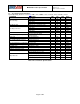
MPU-9250 Product Specification Document Number: PS-MPU-9250A-01 Revision: 1.0 Release Date: 01/17/2014 CONTENTS 1 2 3 4 DOCUMENT INFORMATION ............................................................................................................ 4 1.1 R EVISION HISTORY .................................................................................................................... 4 1.2 PURPOSE AND S COPE .......................................................................................
MPU-9250 Product Specification Document Number: PS-MPU-9250A-01 Revision: 1.0 Release Date: 01/17/2014 4.14 MPU-9250 SOLUTION USING SPI INTERFACE.............................................................................. 26 4.15 CLOCKING .............................................................................................................................. 26 4.16 SENSOR DATA R EGISTERS .......................................................................................................
MPU-9250 Product Specification 1 Document Information 1.1 Revision History Revision Date Revision Description 01/17/14 1.0 Initial Release Page 4 of 42 Document Number: PS-MPU-9250A-01 Revision: 1.
Document Number: PS-MPU-9250A-01 Revision: 1.0 Release Date: 01/17/2014 MPU-9250 Product Specification 1.2 Purpose and Scope This document is a preliminary product specification, providing a description, specifications, and design related information on the MPU-9250™ MotionTracking device. The device is housed in a small 3x3x1mm QFN package. Specifications are subject to change without notice. Final specifications will be updated based upon characterization of production silicon.
MPU-9250 Product Specification Document Number: PS-MPU-9250A-01 Revision: 1.0 Release Date: 01/17/2014 2 Features 2.1 Gyroscope Features The triple-axis MEMS gyroscope in the MPU-9250 includes a wide range of features: • • • • • • Digital-output X-, Y-, and Z-Axis angular rate sensors (gy roscopes) wit h a user-programmable fullscale range of ±250, ±500, ±1000, and ±2000°/sec and integrated 16-bit ADCs Digitally-programmable low-pass filter Gyroscope operating current: 3.
MPU-9250 Product Specification • • • 2.5 Document Number: PS-MPU-9250A-01 Revision: 1.
MPU-9250 Product Specification Document Number: PS-MPU-9250A-01 Revision: 1.0 Release Date: 01/17/2014 3 Electrical Characteristics 3.1 Gyroscope Specifications Typical Operating Circuit of section 4.2, VDD = 2.5V, VDDIO = 2.5V, TA=25°C, unless otherwise noted.
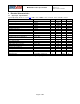
Document Number: PS-MPU-9250A-01 Revision: 1.0 Release Date: 01/17/2014 MPU-9250 Product Specification 3.2 Accelerometer Specifications Typical Operating Circuit of section 4.2, VDD = 2.5V, VDDIO = 2.5V, TA=25°C, unless otherwise noted. PARAMETER Full-Scale Range ADC Word Length Sensitivity Scale Factor Initial Tolerance Sensitivity Change vs. Temperature Nonlinearity Cross-Axis Sensitivity Zero-G Initial Calibration Tolerance Zero-G Level Change vs.
MPU-9250 Product Specification Document Number: PS-MPU-9250A-01 Revision: 1.0 Release Date: 01/17/2014 3.3 Magnetometer Specifications Typical Operating Circuit of section 4.2, VDD = 2.5V, VDDIO = 2.5V, TA=25°C, unless otherwise noted. PARAMETER CONDITIONS MIN MAGNETOMETER SENSITIVITY Full-Scale Range ADC Word Length Sensitivity Scale Factor ZERO-FIELD OUTPUT Initial Calibration Tolerance Page 10 of 42 TYP MAX UNITS ±4800 14 0.
Document Number: PS-MPU-9250A-01 Revision: 1.0 Release Date: 01/17/2014 MPU-9250 Product Specification 3.4 Electrical Specifications 3.4.1 D.C. Electrical Characteristics Typical Operating Circuit of section 4.2, VDD = 2.5V, VDDIO = 2.5V, TA=25°C, unless otherwise noted. PARAMETER CONDITIONS MIN TYP MAX Units VDD 2.4 VDDIO 1.71 2.5 3.6 V 1.
MPU-9250 Product Specification 3.4.2 Document Number: PS-MPU-9250A-01 Revision: 1.0 Release Date: 01/17/2014 A.C. Electrical Characteristics Typical Operating Circuit of section 4.2, VDD = 2.5V, VDDIO = 2.5V, TA=25°C, unless otherwise noted. Param eter Supply Ramp Time Conditions Monotonic ramp.
MPU-9250 Product Specification Frequency Variation over Temperature CLK_SEL=1,2,3,4,5; 25°C CLK_SEL=0,6 CLK_SEL=1,2,3,4,5 -1 -10 Table 4 A.C. Electrical Characteristics Page 13 of 42 Document Number: PS-MPU-9250A-01 Revision: 1.
Document Number: PS-MPU-9250A-01 Revision: 1.0 Release Date: 01/17/2014 MPU-9250 Product Specification 3.4.3 Other Electrical Specifications Typical Operating Circuit of section 4.2, VDD = 2.5V, VDDIO = 2.5V, TA=25°C, unless otherwise noted.
Document Number: PS-MPU-9250A-01 Revision: 1.0 Release Date: 01/17/2014 MPU-9250 Product Specification 3.5 I2C Timing Characterization Typical Operating Circuit of section 4.2, VDD = 2.4V to 3.6V, VDDIO = 1.71 to VDD, TA=25°C, unless otherwise noted. Param eters I2C TIMING f SCL, SCL Clock Frequency tHD.ST A , (Repeated) START Condition Hold Time tLOW , SCL Low Period tHIGH, SCL High Period tSU.ST A , Repeated START Condition Setup Time tHD.DAT , SDA Data Hold Time tSU.
Document Number: PS-MPU-9250A-01 Revision: 1.0 Release Date: 01/17/2014 MPU-9250 Product Specification 3.6 SPI Timing Characterization Typical Operating Circuit of section 4.2, VDD = 2.4V to 3.6V, VDDIO = 1.71V to VDD, TA=25°C, unless otherwise noted. Param eters Conditions Min Typical Max Units 1 MHz Notes SPI TIMING f SCLK , SCLK Clock Frequency tLOW , SCLK Low Period 400 ns tHIGH, SCLK High Period 400 ns tSU.CS , CS Setup Time 8 ns tHD.CS , CS Hold Time 500 ns tSU.
Document Number: PS-MPU-9250A-01 Revision: 1.0 Release Date: 01/17/2014 MPU-9250 Product Specification tSU.SDI, SDI Setup Time 0 ns tHD.SDI, SDI Hold Time 1 ns tVD.SDO, SDO Valid Time Cload = 20pF 25 tDIS.SDO, SDO Output Disable Time ns 25 ns Table 8 fCLK = 20MHz Note: 1.
Document Number: PS-MPU-9250A-01 Revision: 1.0 Release Date: 01/17/2014 MPU-9250 Product Specification 3.7 Absolute Maximum Ratings Stress above those listed as “Absolute Maximum Ratings” may cause permanent damage to the device. These are stress ratings only and functional operation of the device at these conditions is not implied. Exposure to the absolute maximum ratings conditions for extended periods may affect device reliability.
Document Number: PS-MPU-9250A-01 Revision: 1.0 Release Date: 01/17/2014 MPU-9250 Product Specification 4 Applications Information Pin Out and Signal Description Pin Num ber 1 Pin Nam e RESV Pin Description Reserved. Connect to VDDIO.
Document Number: PS-MPU-9250A-01 Revision: 1.0 Release Date: 01/17/2014 MPU-9250 Product Specification Typical Operating Circuit RESV 1 18 NC 2 NC 3 NC GND RESV 19 20 21 RESV AUX_DA SDA / SDI nCS 22 23 24 RESV RESV 19 20 21 nCS SCL / SCLK AUX_DA 22 23 SDA / SDI 24 SCLK SDI SCL / SCLK nCS VDDIO SCL SDA GND RESV 1 18 17 NC NC 2 17 NC 16 NC NC 3 4 15 NC NC 4 NC 5 14 NC NC 5 14 NC NC 6 13 VDD NC 6 13 VDD C3, 10 nF AD0 2.4 – 3.3VDC 12 C2, 0.
Document Number: PS-MPU-9250A-01 Revision: 1.0 Release Date: 01/17/2014 MPU-9250 Product Specification 4.
MPU-9250 Product Specification Document Number: PS-MPU-9250A-01 Revision: 1.0 Release Date: 01/17/2014 4.5 Overview The MPU-9250 is comprised of the following key blocks and functions: • • • • • • • • • • • • • • 4.
MPU-9250 Product Specification Document Number: PS-MPU-9250A-01 Revision: 1.0 Release Date: 01/17/2014 rd gyroscopes, magnet ometers and additional 3 party sensors, and processes the data. The resulting data can be read from the DMP’s registers, or can be buffered in a FIFO. The DMP has access to one of the MPU’s external pins, which can be used for generating interrupts. This pin (pin 12) should be connected t o a pin on the host processor that can wake the host from suspend mode.
MPU-9250 Product Specification Document Number: PS-MPU-9250A-01 Revision: 1.0 Release Date: 01/17/2014 Pass-Through mode is useful for c onfiguring the external sensors, or for keeping the MPU-9250 in a low-power mode when only the external sensors are used. In this mode, the system processor can 2 still access MPU-9250 data through the I C interface. Pass-Through mode is also used to access the AK8963 magnetometer directly from the host.
Document Number: PS-MPU-9250A-01 Revision: 1.0 Release Date: 01/17/2014 MPU-9250 Product Specification 4.13 MPU-9250 Solution Using I2C Interface 2 In the figure below, the system processor is an I C master to the MPU-9250. In addition, the MPU-9250 is an 2 rd 2 I C master to the optional external 3 party sensor. The MP U-9250 has limited capabilities as an I C Master, and depends on the system processor to manage the initial configuration of any auxiliary sensors.
Document Number: PS-MPU-9250A-01 Revision: 1.0 Release Date: 01/17/2014 MPU-9250 Product Specification 4.14 MPU-9250 Solution Using SPI Interface In the figure below, the system processor is a SPI master to the MPU-9250. The CS, SDO, SCLK, and SDI 2 signals are used for SPI communications.
MPU-9250 Product Specification Document Number: PS-MPU-9250A-01 Revision: 1.0 Release Date: 01/17/2014 Allowable internal sources for generating the internal clock are: • • An internal relaxation oscillator Any of the X, Y, or Z gyros (MEMS oscillators with a variation of ±1% over temperature) Selection of the source for generating the internal synchronous clock depends on the requirements for power consumption and clock accuracy. These requirements will most likely vary by mode of operation.
MPU-9250 Product Specification Document Number: PS-MPU-9250A-01 Revision: 1.0 Release Date: 01/17/2014 4.20 Bias and LDO The bias and LDO section generates the int ernal supply and the reference voltages and currents required by the MPU-9250. Its two inputs are an unregulated VDD and a V DDIO logic reference supply voltage. The LDO output is bypassed by a capacitor at REGOUT. For further details on the capacitor, please refer to the Bill of Materials for External Components. 4.
MPU-9250 Product Specification Document Number: PS-MPU-9250A-01 Revision: 1.0 Release Date: 01/17/2014 5 Advanced Hardware Features The MPU-9250 includes advanced hardware features that can be enabled and disabled through simple hardware register settings. The advanced hardware features are not initially enabled after device power up. These features must be individually enabled and configured.
MPU-9250 Product Specification Document Number: PS-MPU-9250A-01 Revision: 1.0 Release Date: 01/17/2014 6 Programmable Interrupts The MPU-9250 has a programmable interrupt system which can generate an interrupt signal on the INT pin. Status flags indicate the source of an interrupt. Interrupt sources may be enabled and disabled individually.
MPU-9250 Product Specification Document Number: PS-MPU-9250A-01 Revision: 1.
MPU-9250 Product Specification Document Number: PS-MPU-9250A-01 Revision: 1.0 Release Date: 01/17/2014 7 Digital Interface 7.1 I2C and SPI Serial Interfaces 2 The internal registers and memory of the MPU-9250 can be accessed using either I C at 400 kHz or SPI at 1MHz. SPI operates in four-wire mode.
MPU-9250 Product Specification Document Number: PS-MPU-9250A-01 Revision: 1.0 Release Date: 01/17/2014 SDA SCL S P START condition STOP condition START and STOP Conditions Data Format / Ack nowledge 2 I C data bytes are defined to be 8-bits long. There is no restriction to the number of bytes transmitted per data transfer. Each byte transferred must be followed by an acknowledge (ACK ) signal.
Document Number: PS-MPU-9250A-01 Revision: 1.0 Release Date: 01/17/2014 MPU-9250 Product Specification Communications After beginning communications with the S TA RT condition (S), the master sends a 7-bit slave address th followed by an 8 bit, the read/write bit. The read/writ e bit indicates whether the master is receiving data from or is writing to the slave device. Then, the master releases the SDA line and waits for the acknowledge signal (ACK ) from the slave device.
MPU-9250 Product Specification Document Number: PS-MPU-9250A-01 Revision: 1.0 Release Date: 01/17/2014 2 To read the internal MP U-9250 registers, the master sends a start condition, followed by the I C address and a writ e bit, and then t he register address that is going to be read. Upon receiving the A CK signal from the MPU-9250, the master transmits a start signal followed by the slave address and read bit. As a result, the MPU-9250 sends an ACK signal and the data.
Document Number: PS-MPU-9250A-01 Revision: 1.0 Release Date: 01/17/2014 MPU-9250 Product Specification 7.5 SPI Interface SPI is a 4-wire synchronous serial interface that uses two control lines and two data lines. The MPU-9250 always operates as a Slave device during standard Master-Slave SPI operation. With respect to the Master, the Serial Clock output (SCLK ), the Serial Data Output (SDO) and the Serial Data Input (SDI) are shared among the Slave devices.
MPU-9250 Product Specification Document Number: PS-MPU-9250A-01 Revision: 1.0 Release Date: 01/17/2014 8 Serial Interface Considerations 8.1 MPU-9250 Supported Interfaces 2 The MPU-9250 supports I C communications on both its primary (microprocessor) serial interface and its auxiliary interface. The MPU-9250’s I/O logic levels are set to be VDDIO. 2 The figure below depicts a sample circuit of MP U-9250 with a third party sensor attached to the auxiliary I C bus.
MPU-9250 Product Specification Document Number: PS-MPU-9250A-01 Revision: 1.0 Release Date: 01/17/2014 9 Assembly This section provides general guidelines for assembling InvenS ense Micro Electro-Mechanical Systems (MEMS) devices packaged in quad flat no-lead package (QFN) surface mount integrated circuits. 9.1 Orientation of Axes The diagram below shows the orientation of the axes of sensitivity and the polarity of rotation. Not e the pin 1 identifier (•) in the figure.
Document Number: PS-MPU-9250A-01 Revision: 1.
MPU-9250 Product Specification Document Number: PS-MPU-9250A-01 Revision: 1.
MPU-9250 Product Specification Document Number: PS-MPU-9250A-01 Revision: 1.0 Release Date: 01/17/2014 11 Reliability 11.1 Qualification Test Policy InvenSense’s products complete a Qualification Test Plan before being released to production. The Qualification Test Plan for the MPU-9250 followed the JEDE C JESD 47I Standard, “Stress-Test-Driven Qualification of Integrated Circuits,” with the individual tests described below. 11.
MPU-9250 Product Specification Document Number: PS-MPU-9250A-01 Revision: 1.