
Data Sheet


HX711
AVIA SEMICONDUCTOR
5
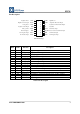
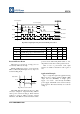
DOUT
PD_SCK 12
MSB
LSB
24 25
Next Conversion
:CH.A, Gain:128
Current Output Data
Next Output Data
34
PD_SCK
12 24 25
Next Conversion
:CH.B, Gain:32
34
26
PD_SCK
12 24 25
Next Conversion
:CH.B, Gain:64
34
26 27
Fig.2 Data output, input and gain selection timing and control
T
1
T
2
T
3
T
4
One conversion period
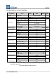
Symbol Note MIN TYP MAX Unit
T
1
DOUT falling edge to PD_SCK rising edge 0.1
µs
T
2
PD_SCK rising edge to DOUT data ready 0.1
µ
s
T
3
PD_SCK high time 0.2 1 50
µs
T
4
PD_SCK low time 0.2 1
µ
s
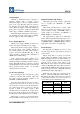
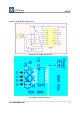
Reset and Power-Down
When chip is powered up, on-chip power on
rest circuitry will reset the chip.
Pin PD_SCK input is used to power down the
HX711. When PD_SCK Input is low, chip is in
normal working mode.
60
µ
s
Power down:
PD_SCK
Power down
Normal
Fig.3 Power down control
When PD_SCK pin changes from low to high
and stays at high for longer than 60
µs
, HX711
enters power down mode (Fig.3). When internal
regulator is used for HX711 and the external
transducer, both HX711 and the transducer will be
powered down. When PD_SCK returns to low,
chip will reset and enter normal operation mode.
After a reset or power-down event, input
selection is default to Channel A with a gain of
128.
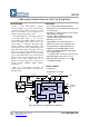
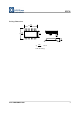
Application Example
Fig.1 is a typical weigh scale application using
HX711. It uses on-chip oscillator (XI=0), 10Hz
output data rate (RATE=0). A Single power
supply (2.7~5.5V) comes directly from MCU
power supply. Channel B can be used for battery
level detection. The related circuitry is not shown
on Fig. 1.