
Manual


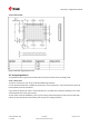


Table Of Contents
- Title
- Contents
- 1 Integration manual structure
- 2 System description
- 3 Receiver functionality
- 3.1 Receiver configuration
- 3.1.1 Changing the receiver configuration
- 3.1.2 Default GNSS configuration
- 3.1.3 Default interface settings
- 3.1.4 Basic receiver configuration
- 3.1.5 Differential timing mode configuration
- 3.1.6 Legacy configuration interface compatibility
- 3.1.7 Navigation configuration
- 3.2 Geofencing
- 3.3 Logging
- 3.4 Communication interfaces
- 3.5 Predefined PIOs
- 3.6 Antenna supervisor
- 3.7 Multiple GNSS assistance (MGA)
- 3.8 Clocks and time
- 3.9 Timing functionality
- 3.10 Security
- 3.11 u-blox protocol feature descriptions
- 3.12 Forcing a receiver reset
- 3.13 Firmware upload
- 3.1 Receiver configuration
- 4 Design
- 5 Product handling
- Appendix
- Related documents
- Revision history
- Contact

ZED-F9T-Integration manual
• Bias-t inductor must be L1 and L2 band frequency selected with high impedance in the GNSS
band.
• Ensure RF trace is tuned for 50 Ω to ensure L1 and L2 bandwidth.
4.8.5 Ground pads
Ensure the ground pads of the module are connected to ground.
4.8.6 Schematic design
For a minimal design with the ZED-F9T GNSS modules, consider the following functions and pins:
• Connect the power supply to VCC and V_BCKP.
• V_USB: If USB is used it is recommended V_USB is to be powered as per USB self-powered mode
specification.
• If USB is not used connect V_USB to ground.
• Ensure an optimal ground connection to all ground pins of the ZED-F9T GNSS module.
• Choose the required serial communication interfaces (UART, USB, SPI or I2C) and connect the
appropriate pins to your application.
• If you need hot or warm start in your application, connect a backup battery to V_BCKP.
• Antenna bias is required, see ZED-F9T antenna bias section.
4.8.7 Layout design-in guideline
• Is the receiver placed away from heat sources?
• Is the receiver placed away from air-cooling sources?
• Is the receiver shielded by a cover/case to prevent the effects of air currents and rapid
environmental temperature changes?
• Is the receiver placed as recommended in the Layout and Layout guidance?
• Assure a low serial resistance on the VCC power supply line (choose a line width > 400 um).
• Keep the power supply line as short as possible.
• Add a ground plane underneath the module to reduce interference. This is especially important
for the RF input line.
• For improved shielding, add as many vias as possible around the micro strip/co-planar
waveguide, around the serial communication lines, underneath the module, etc.
UBX-19005590 - R05
4 Design Page 78 of 87
C1-Public Early production information