
Manual


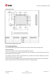


Table Of Contents
- Title
- Contents
- 1 Integration manual structure
- 2 System description
- 3 Receiver functionality
- 3.1 Receiver configuration
- 3.1.1 Changing the receiver configuration
- 3.1.2 Default GNSS configuration
- 3.1.3 Default interface settings
- 3.1.4 Basic receiver configuration
- 3.1.5 Differential timing mode configuration
- 3.1.6 Legacy configuration interface compatibility
- 3.1.7 Navigation configuration
- 3.2 Geofencing
- 3.3 Logging
- 3.4 Communication interfaces
- 3.5 Predefined PIOs
- 3.6 Antenna supervisor
- 3.7 Multiple GNSS assistance (MGA)
- 3.8 Clocks and time
- 3.9 Timing functionality
- 3.10 Security
- 3.11 u-blox protocol feature descriptions
- 3.12 Forcing a receiver reset
- 3.13 Firmware upload
- 3.1 Receiver configuration
- 4 Design
- 5 Product handling
- Appendix
- Related documents
- Revision history
- Contact

ZED-F9T-Integration manual
When an RF input connector is employed this can provide a conduction path for harmful or
destructive electrical signals. If this is a likely factor the RF input should be protected accordingly.
Additional points on the RF input
• What is the expected quality of the signal source (antenna)?
• What is the external active antenna signal power?
• What is the bandwidth and filtering of the external active antenna?
• Does the external antenna and filtering components meet the group delay variation
requirements? This is critical for RTK.
Are destructive RF power levels expected to reach the RF input? Is interference from wireless
transmitters expected?
• What are the characteristics of these signals (duty cycle, frequency range, power range,
spectral purity)?
• What is the expected GNSS performance under interference conditions?
Is there a risk of RF input exposure to excessive ESD stress?
• In the field: Can the user access the antenna connector?
• PCB / system assembly: Is there risk that statically charged parts (e.g. patch antennas) may be
discharged through the RF input?
The following subsections provide several options addressing the various questions above:
In some applications, such as cellular transceivers, interference signals may exceed the
maximum power rating of the RF_IN input. To avoid device destruction use of external input
protection is mandatory.
During assembly of end-user devices which contain passive patch antennas, an ESD
discharge may occur during production when pre-charged antennas are soldered to the
GNSS receiver board. In such cases, use of external protection in front of RF_IN is mandatory
to avoid device destruction.
ESD discharge cannot be avoided during assembly and / or field use. Note that SAW filters are
susceptible to ESD damage. To provide additional robustness an ESD protection diode may be
placed at the antenna RF connector to GND.
4.8.4 Antenna/RF input
Check RF input requirements and schematic:
• An OEM active antenna module that meets our requirements should be used if there is a need
to integrate the antenna.
• The total maximum noise figure including external LNA (or the LNA in the active antenna)
should be around 3 dB.
• Ensure active antenna gain is ideally between 30 - 40 dB gain.
• Make sure the antenna is not placed close to noisy parts of the circuitry and does not face any
other noisy elements (for example micro-controller, display).
• Signal levels above 40 C/N0 average are required for optimal RTK performance.
• If a patch type antenna is used, an antenna ground plane with minimum 100 - 150 mm
diameter is required.
• Ensure antenna supports both L1 and L2 bands.
• Ensure antenna element gain is between 2 and 3 dBic typical for L1 and L2 bands.
• Ensure the group delay variation including active antenna is 10 ns max at each GNSS system
bandwidth. Note: Inter-signal requirement 50 ns max.
• ESD protection on the RF input is mandatory.
UBX-19005590 - R05
4 Design Page 77 of 87
C1-Public Early production information