
Manual


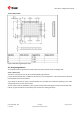


Table Of Contents
- Title
- Contents
- 1 Integration manual structure
- 2 System description
- 3 Receiver functionality
- 3.1 Receiver configuration
- 3.1.1 Changing the receiver configuration
- 3.1.2 Default GNSS configuration
- 3.1.3 Default interface settings
- 3.1.4 Basic receiver configuration
- 3.1.5 Differential timing mode configuration
- 3.1.6 Legacy configuration interface compatibility
- 3.1.7 Navigation configuration
- 3.2 Geofencing
- 3.3 Logging
- 3.4 Communication interfaces
- 3.5 Predefined PIOs
- 3.6 Antenna supervisor
- 3.7 Multiple GNSS assistance (MGA)
- 3.8 Clocks and time
- 3.9 Timing functionality
- 3.10 Security
- 3.11 u-blox protocol feature descriptions
- 3.12 Forcing a receiver reset
- 3.13 Firmware upload
- 3.1 Receiver configuration
- 4 Design
- 5 Product handling
- Appendix
- Related documents
- Revision history
- Contact

ZED-F9T-Integration manual
Figure 42: RF input trace
The RF_IN trace on the top layer should be referenced to a suitable ground layer.
4.7.4.2 Vias for the ground pads
The ground pads under the ZED-F9T high accuracy timing receiver need to be grounded with vias to
the lower ground layer of the PCB. A solid ground layer fill on the top layer of the PCB is recommended.
This is shown in the figure below.
Figure 43: Top layer fill and vias
4.7.4.3 VCC pads
The VCC pads for the ZED-F9T high accuracy timing receiver must have as low impedance as
possible with large vias to the lower power layer of the PCB. The VCC pads need a large combined
pad and the de-coupling capacitors must be placed as close as possible. This is shown in the figure
below.
UBX-19005590 - R05
4 Design Page 75 of 87
C1-Public Early production information