
Manual
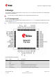


Table Of Contents
- Title
- Contents
- 1 Integration manual structure
- 2 System description
- 3 Receiver functionality
- 3.1 Receiver configuration
- 3.1.1 Changing the receiver configuration
- 3.1.2 Default GNSS configuration
- 3.1.3 Default interface settings
- 3.1.4 Basic receiver configuration
- 3.1.5 Differential timing mode configuration
- 3.1.6 Legacy configuration interface compatibility
- 3.1.7 Navigation configuration
- 3.2 Geofencing
- 3.3 Logging
- 3.4 Communication interfaces
- 3.5 Predefined PIOs
- 3.6 Antenna supervisor
- 3.7 Multiple GNSS assistance (MGA)
- 3.8 Clocks and time
- 3.9 Timing functionality
- 3.10 Security
- 3.11 u-blox protocol feature descriptions
- 3.12 Forcing a receiver reset
- 3.13 Firmware upload
- 3.1 Receiver configuration
- 4 Design
- 5 Product handling
- Appendix
- Related documents
- Revision history
- Contact

ZED-F9T-Integration manual
4 Design
This section provides information to help carry out a successful schematic and PCB design
integrating the ZED-F9T.
Do not load Pin 4 (ANT_DETECT) with a capacitance more than 1 nF.
4.1 Pin assignment
The pin assignment of the ZED-F9T module is shown in Figure 30. The defined configuration of the
PIOs is listed in Table 25.
The ZED-F9T is an LGA package with the I/O on the outside edge and central ground pads.
Figure 30: ZED-F9T pin assignment
Pin no. Name I/O Description
1 GND - Ground
2 RF_IN I RF input
3 GND - Ground
4 ANT_DETECT I Active antenna detect - default active high
5 ANT_OFF O External LNA disable - default active high
6 ANT_SHORT_N I Active antenna short detect - default active low
UBX-19005590 - R05
4 Design Page 61 of 87
C1-Public Early production information