
Data Sheet


Copyright © 2013 Future Technology Devices International Limited 9
FT231X USB TO FULL HANDSHAKE UART IC
Datasheet
Version 1.2
Document No.: FT_000565 Clearance No.: FTDI# 261
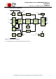
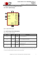
3.2 20-LD SSOP Package
RXD
4
RI#
5
GND
6
DSR#
7
DCD#
8
CTS#
9
CBUS2
10
USBDP
11
USBDM
12
3V3OUT
13
RESET#
14
VCC
15
GND
16
CBUS1
17
CBUS0
18
CBUS3
19
TXD
20
DTR#
1
RTS#
2
VCCIO
3
Figure 3.2 SSOP Schematic Symbol
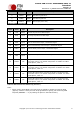
3.2.1 SSOP Package PinOut Description
Note: # denotes an active low signal.
Pin No.
Name
Type
Description
15
**
VCC
POWER
Input
5 V or 3V3 supply to IC
3
VCCIO
POWER
Input
1V8 – 3V3 supply for the IO cells
13
**
3V3OUT
POWER
Output
3V3 output at 50mA. May be used to power VCCIO.
When VCC is 3V3, pin 13 is an input pin.
6, 16
GND
POWER
Input
0V Ground input.
Table 3.4 Power and Ground
** If VCC is 3V3 then 3V3OUT must also be driven with 3V3 input
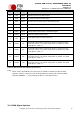
Pin No.
Name
Type
Description
12
USBDM
INPUT
USB Data Signal Minus.
11
USBDP
INPUT
USB Data Signal Plus.
14
RESET#
INPUT
Reset input (active low).
Table 3.5 Common Function pins