
Data Sheet


Copyright © 2013 Future Technology Devices International Limited 7
FT231X USB TO FULL HANDSHAKE UART IC
Datasheet
Version 1.2
Document No.: FT_000565 Clearance No.: FTDI# 261
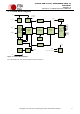
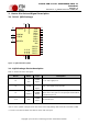
3 Device Pin Out and Signal Description
3.1 20-LD QFN Package
VCCIO
20
RI#
2
DTR#
18
GND
3
DSR#
4
RTS#
19
CTS#
6
CBUS2
7
USBDP
8
USBDM
9
3V3OUT
10
RESET#
11
VCC
12
CBUS1
14
CBUS0
15
GND
13
TXD
17
DCD#
5
RXD
1
CBUS3
16
GND
21
Figure 3.1 QFN Schematic Symbol
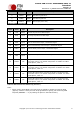
3.1.1 QFN Package PinOut Description
Note: # denotes an active low signal.
Pin No.
Name
Type
Description
12
**
VCC
POWER
Input
5 V or 3V3 supply to IC
20
VCCIO
POWER
Input
1V8 – 3V3 supply for the IO cells
10
**
3V3OUT
POWER
Output
3V3 output at 50mA. May be used to power VCCIO.
When VCC is 3V3; pin 10 is an input pin and should be
connected to pin 12.
3, 13
GND
POWER
Input
0V Ground input.
Table 3.1 Power and Ground
*Pin 21 on the symbol is the pad under the centre of the chip package and should be connected to GND
** If VCC is 3V3 then 3V3OUT must also be driven with 3V3 input