
Data Sheet


Copyright © 2013 Future Technology Devices International Limited 30
FT231X USB TO FULL HANDSHAKE UART IC
Datasheet
Version 1.2
Document No.: FT_000565 Clearance No.: FTDI# 261
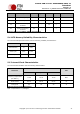
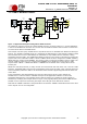
X-Chip Pin Function
EEPROM Setting
CBUS0
CBUS1
CBUS2
BCD#
PWREN#
SLEEP#
Battery Options
Battery Charger Enable
Force Power Enable
De-acticate Sleep
X
X
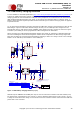
PWREN#
GND
CBUS2
10
DP
DM
3V3OUT
RESET#
VCC
GND
CBUS1
17
CBUS0
18
VCCIO
FT231X
BCD#
SLEEP#
GND
GND
0.1uF
0.1uF
GND
GND
600R/2A
10nF
VBUS 3V3OUT
0.1uF
0R
GNDSLD GND
27R
27R
VBUS
1
D-
2
D+
3
GND
5
ID
4
CN USB
3V3OUT 3V3OUTVBUS VBUS
N.F.
1K5 - 1%16K5 1%
GND
BCD#
4K32 1%
PWREN#
1A when connected to a dedicated charger port
0.4A when enumerated
0A when in sleep
0.1A when not enumerated and not in sleep
VCC
2
FAULT
3
TIMER
4
GND
5
NTC
6
PROG
7
SHDN
8
BAT
9
ACPR
10
CHRG
1
GND
11
LTC4053EDD
GND
4.7uF
0.1uF
GND
VBUSVBUS
GND
VBATT
GND
GND
1
TB3.5mm
NTC
0.1uF
GND
VBUS
1uF
1R
GND
VBUS
2K2
GND
JP1
1-2
2-3
NCT Enabled
NCT Available
JP1
SIP-3
NTC
GND
NCT Disabled (Default)
JUMPER-2mm
4K32 1%
+
-
NCT
SLEEP#
Figure 7.6 USB Battery Charging Detection (3 pin)
To calculate the equivalent resistance on the LTC4053 PROG pin select a charge current, then Res =
1500V/I
chg
For more configuration options of the LTC4053 refer to:
AN_175_Battery Charging Over USB
Note: If the FT231X is connected to a standard host port such that the device is enumerated the battery
charge detection signal is inactive as the device will not be in suspend.
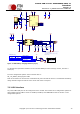
7.5 LED Interface
Any of the CBUS I/O pins can be configured to drive an LED. The FT231X has 3 configuration options for
driving LEDs from the CBUS. These are TXLED#, RXLED#, and TX&RXLED#. Refer to Section 3.3 for
configuration options.