
Data Sheet


Copyright © 2013 Future Technology Devices International Limited 29
FT231X USB TO FULL HANDSHAKE UART IC
Datasheet
Version 1.2
Document No.: FT_000565 Clearance No.: FTDI# 261
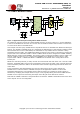
X-Chip Pin Function
EEPROM Setting
CBUS5
CBUS6
SLEEP#
PWREN#
Battery Options
Battery Charger Enable
Force Power Enable
De-acticate Sleep
X
X
X
SLEEP#
PWREN#
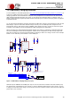
DP
DM
3V3OUT
VCORE
RESET#
VCC
CBUS6
CBUS5
VCCIO
U1
FT231X
0.4A when connected to a dedicated charger port
GND
GND
0.1uF 0.1uF
GND
GND
600R/2A
10nF
VBUS 3V3OUT
0.1uF
0R
GNDSLD GND
27R
27R
VBUS
1
D-
2
D+
3
GND
5
ID
4
CN USB
3V3OUT 3V3OUTVBUS VBUS
N.F.
16K5 1%
GND
4K32 1%
PWREN#
0.4A when enumerated
0A when in sleep mode
0.1A when not enumerated and not in sleep mode
VCC
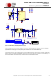
2
FAULT
3
TIMER
4
GND
5
NTC
6
PROG
7
SHDN
8
BAT
9
ACPR
10
CHRG
1
GND
11
LTC4053EDD
GND
4.7uF
0.1uF
GND
VBUSVBUS
GND
VBATT
GND
GND
1
TB3.5mm
NTC
0.1uF
GND
VBUS
1uF
1R
GND
VBUS
2K2
GND
JP1
1-2
2-3
NCT Enabled
NCT Available
JP1
SIP-3
NTC
GND
NCT Disabled (Default)
JUMPER-2mm
4K32 1%
+
-
NCT
SLEEP#
Figure 7.5 USB Battery Charging Detection (2 pin)
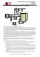
In the example above the FT231X SLEEP pin is used to enable/disable the LTC4053, while the PWREN#
signal alters the charging current by altering the resistance on the LTC4053 PROG pin.
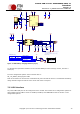
A third option shown in the example below uses the SLEEP signal from the FT231X to enable / disable the
battery charger. The BCD# and PWREN# signals are then used to alter the resistance on the PROG pin of
the LTC4053 which controls the charge current drawn from the USB connector.