
Data Sheet


Copyright © 2013 Future Technology Devices International Limited 10
FT231X USB TO FULL HANDSHAKE UART IC
Datasheet
Version 1.2
Document No.: FT_000565 Clearance No.: FTDI# 261
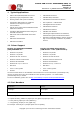
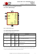
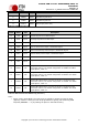
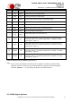
Pin No.
Name
Type
Description
20
TXD
Output
Transmit Asynchronous Data Output.
4
RXD
Input
Receiving Asynchronous Data Input.
2
RTS#
Output
Request to Send Control Output / Handshake Signal.
9
CTS#
Input
Clear To Send Control Input / Handshake Signal.
1
DTR#
Output
Data Terminal Ready Control Output / Handshake Signal.
7
DSR#
Input
Data Set Ready Control Input / Handshake Signal.
8
DCD#
Input
Data Carrier Detect Control Input.
5
RI#
Input
Ring Indicator input for remote wake up.
18
CBUS0
I/O
Configurable CBUS I/O Pin. Function of this pin is configured in the
device MTP memory. The default configuration is TXDEN. See CBUS
Signal Options, Table 3.7.
17
CBUS1
I/O
Configurable CBUS I/O Pin. Function of this pin is configured in the
device MTP memory. The default configuration is RXLED#. See CBUS
Signal Options, Table 3.7.
10
CBUS2
I/O
Configurable CBUS I/O Pin. Function of this pin is configured in the
device MTP memory. The default configuration is TXLED#. See CBUS
Signal Options, Table 3.7.
19
CBUS3
I/O
Configurable CBUS I/O Pin. Function of this pin is configured in the
device MTP memory. The default configuration is SLEEP#. See CBUS
Signal Options, Table 3.7.
Table 3.6 UART Interface and CBUS Group (see note 1)
Notes:
1 When used in Input Mode, the input pins are pulled to VCCIO via internal 75kΩ
(approx) resistors. These pins can be programmed to gently pull low during USB
suspend (PWREN# = “1”) by setting an option in the MTP memory.
3.3 CBUS Signal Options