
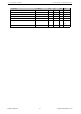
Data Sheet

7.2 Community Resources 7 SUPPORTED RESOURCES
Note:
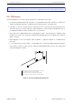
The examples illustrated in Figure 6 are not of actual scale. It is suggested that users take a human fingertip as reference.
A.2. PCB Layout
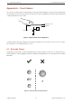
The recommendations for correctly routing sensing tracks of electrodes are as follows:
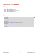
• Close proximity between electrodes may lead to crosstalk between electrodes and false touch detections.
The distance between electrodes should be at least twice the thickness of the panel used.
• The width of a sensor track creates parasitic capacitance, which could vary with manufacturing processes.
The thinner the track is, the less capacitive coupling it generates. The track width should be kept as thin as
possible and the length should not exceed 10cm to accommodate.
• We should avoid coupling between lines of high frequency signals. The sensing tracks should be routed
parallel to each other on the same layer and the distance between the tracks should be at least twice the
width of the track.
• When designing a touch sensor device, there should be no components adjacent to or underneath the
electrodes.
• Do not ground the touch sensor device. It is preferable that no ground layer be placed under the device,
unless there is a need to isolate it. Parasitic capacitance generated between the touch sensor device and
the ground degrades sensitivity.
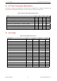
2
1
3
1
Distance between electrodes - Twice the thickness of the panel
2
Distance between tracks - Twice the track width
3
Width of the track (electrode wiring) - As thin as possible
4
4
Distance between track and ground plane - 2mm at a minimum
Figure 7: Sensor Track Routing Requirements
Espressif Systems 35 http://www.espressif.com