
Data Sheet

DS18B20
8 of 27
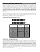
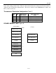
1-WIRE CRC CODE Figure 6
MEMORY
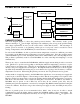
The DS18B20’s memory is organized as shown in Figure 8. The memory consists of a scratchpad RAM
and a nonvolatile, electrically erasable (E
2
) RAM, which stores the high and low temperature triggers TH
and TL, and the configuration register. The scratchpad helps insure data integrity when communicating
over the 1-Wire bus. Data is first written to the scratchpad using the Write Scratchpad [4Eh] command.
It can then be verified by using the Read Scratchpad [BEh] command. After the data has been verified, a
Copy Scratchpad [48h] command will transfer the data to the nonvolatile (E
2
) RAM. This process insures
data integrity when modifying memory. The DS18B20 EEPROM is rated for a minimum of 50,000
writes and 10 years data retention at T = +55°C.
The scratchpad is organized as eight bytes of memory. The first 2 bytes contain the LSB and the MSB of
the measured temperature information, respectively. The third and fourth bytes are volatile copies of TH
and TL and are refreshed with every power-on reset. The fifth byte is a volatile copy of the configuration
register and is refreshed with every power-on reset. The configuration register will be explained in more
detail later in this section of the datasheet. The sixth, seventh, and eighth bytes are used for internal
computations, and thus will not read out any predictable pattern.
It is imperative that one writes TH, TL, and config in succession; i.e. a write is not valid if one writes
only to TH and TL, for example, and then issues a reset. If any of these bytes must be written, all three
must be written before a reset is issued.
There is a ninth byte which may be read with a Read Scratchpad [BEh] command. This byte contains a
cyclic redundancy check (CRC) byte which is the CRC over all of the eight previous bytes. This CRC is
implemented in the fashion described in the section titled “CRC Generation”.
Configuration Register
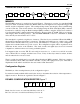
The fifth byte of the scratchpad memory is the configuration register.
It contains information which will be used by the device to determine the resolution of the temperature to
digital conversion. The bits are organized as shown in Figure 7.
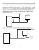
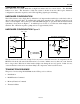
DS18B20 CONFIGURATION REGISTER Figure 7
0R1R0111 1 1
MSb LSb
Bits 0-4 are don’t cares on a write but will always read out “1”.
Bit 7 is a don’t care on a write but will always read out “0”.
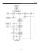
(
MSB
)
XOR
XOR
XOR
(
LSB
)
INPUT