
Data Sheet
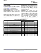
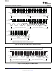
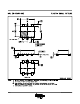

Frame1Two-WireSlaveAddressByte Frame2PointerRegisterByte
1
StartBy
Master
ACKBy
TMP102
ACKBy
TMP102
Frame3Two-WireSlaveAddressByte Frame4DataByte1ReadRegister
StartBy
Master
ACKBy
TMP102
ACKBy
Master
(2)
From
TMP102
1 9 1
9
1 9 1
9
SDA
SCL
0 0 1 R/W
0 0 0 0 0 0 P1 P0
¼
¼
¼
SDA
(Continued)
SCL
(Continued)
SDA
(Continued)
SCL
(Continued)
1 0 0 1
0
A1
(1)
A0
(1)
0
A1
(1)
A0
(1)
R/W D7 D6 D5 D4 D3 D2 D1 D0
Frame5DataByte2ReadRegister
StopBy
Master
ACKBy
Master
(3)
From
TMP102
1
9
D7 D6 D5 D4 D3 D2 D1 D0
StopBy
Master
NOTE: (1)ThevalueofA0andA1aredeterminedbytheADD0pin.
(2)MastershouldleaveSDAhightoterminateasingle-bytereadoperation.
(3)MastershouldleaveSDAhightoterminateatwo-bytereadoperation.
NOTE:(1)ThevalueofA0andA1aredeterminedbytheADD0pin.
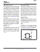
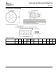
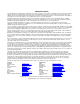
Frame1SMBusALERTResponseAddressByte Frame2SlaveAddressFromTMP102
StartBy
Master
ACKBy
TMP102
From
TMP102
NACKBy
Master
StopBy
Master
1 9 1
9
SDA
SCL
ALERT
0 0 0 1 1 0 0 R/W
1 0 0 1 A1 A0
Status
TMP102
SBOS397B – AUGUST 2007 – REVISED OCTOBER 2008 ...............................................................................................................................................
www.ti.com
Figure 14. Two-Wire Timing Diagram for Read Word Format
Figure 15. Timing Diagram for SMBus ALERT
14 Submit Documentation Feedback Copyright © 2007 – 2008, Texas Instruments Incorporated
Product Folder Link(s): TMP102