
Datasheet


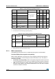
Table Of Contents
- Table 1. Device summary
- 1 Introduction
- 2 Description
- Table 2. STM32F405xx and STM32F407xx: features and peripheral counts (continued)
- 2.1 Full compatibility throughout the family
- 2.2 Device overview
- 2.2.1 ARM® Cortex®-M4 core with FPU and embedded Flash and SRAM
- 2.2.2 Adaptive real-time memory accelerator (ART Accelerator™)
- 2.2.3 Memory protection unit
- 2.2.4 Embedded Flash memory
- 2.2.5 CRC (cyclic redundancy check) calculation unit
- 2.2.6 Embedded SRAM
- 2.2.7 Multi-AHB bus matrix
- 2.2.8 DMA controller (DMA)
- 2.2.9 Flexible static memory controller (FSMC)
- 2.2.10 Nested vectored interrupt controller (NVIC)
- 2.2.11 External interrupt/event controller (EXTI)
- 2.2.12 Clocks and startup
- 2.2.13 Boot modes
- 2.2.14 Power supply schemes
- 2.2.15 Power supply supervisor
- 2.2.16 Voltage regulator
- 2.2.17 Regulator ON/OFF and internal reset ON/OFF availability
- 2.2.18 Real-time clock (RTC), backup SRAM and backup registers
- 2.2.19 Low-power modes
- 2.2.20 VBAT operation
- 2.2.21 Timers and watchdogs
- 2.2.22 Inter-integrated circuit interface (I²C)
- 2.2.23 Universal synchronous/asynchronous receiver transmitters (USART)
- 2.2.24 Serial peripheral interface (SPI)
- 2.2.25 Inter-integrated sound (I2S)
- 2.2.26 Audio PLL (PLLI2S)
- 2.2.27 Secure digital input/output interface (SDIO)
- 2.2.28 Ethernet MAC interface with dedicated DMA and IEEE 1588 support
- 2.2.29 Controller area network (bxCAN)
- 2.2.30 Universal serial bus on-the-go full-speed (OTG_FS)
- 2.2.31 Universal serial bus on-the-go high-speed (OTG_HS)
- 2.2.32 Digital camera interface (DCMI)
- 2.2.33 Random number generator (RNG)
- 2.2.34 General-purpose input/outputs (GPIOs)
- 2.2.35 Analog-to-digital converters (ADCs)
- 2.2.36 Temperature sensor
- 2.2.37 Digital-to-analog converter (DAC)
- 2.2.38 Serial wire JTAG debug port (SWJ-DP)
- 2.2.39 Embedded Trace Macrocell™
- 3 Pinouts and pin description
- 4 Memory mapping
- 5 Electrical characteristics
- 5.1 Parameter conditions
- 5.2 Absolute maximum ratings
- 5.3 Operating conditions
- 5.3.1 General operating conditions
- 5.3.2 VCAP_1/VCAP_2 external capacitor
- 5.3.3 Operating conditions at power-up / power-down (regulator ON)
- 5.3.4 Operating conditions at power-up / power-down (regulator OFF)
- 5.3.5 Embedded reset and power control block characteristics
- 5.3.6 Supply current characteristics
- Table 20. Typical and maximum current consumption in Run mode, code with data processing running from Flash memory (ART accelerator enabled) or RAM
- Table 21. Typical and maximum current consumption in Run mode, code with data processing running from Flash memory (ART accelerator disabled)
- Table 22. Typical and maximum current consumption in Sleep mode
- Table 23. Typical and maximum current consumptions in Stop mode
- Table 24. Typical and maximum current consumptions in Standby mode
- Table 25. Typical and maximum current consumptions in VBAT mode
- Table 26. Typical current consumption in Run mode, code with data processing running from Flash memory, regulator ON (ART accelerator enabled except prefetch), VDD = 1.8 V
- Table 27. Switching output I/O current consumption
- Table 28. Peripheral current consumption
- 5.3.7 Wakeup time from low-power mode
- 5.3.8 External clock source characteristics
- 5.3.9 Internal clock source characteristics
- 5.3.10 PLL characteristics
- 5.3.11 PLL spread spectrum clock generation (SSCG) characteristics
- 5.3.12 Memory characteristics
- 5.3.13 EMC characteristics
- 5.3.14 Absolute maximum ratings (electrical sensitivity)
- 5.3.15 I/O current injection characteristics
- 5.3.16 I/O port characteristics
- 5.3.17 NRST pin characteristics
- 5.3.18 TIM timer characteristics
- 5.3.19 Communications interfaces
- Table 54. I2C analog filter characteristics
- Table 55. SPI dynamic characteristics
- Table 56. I2S dynamic characteristics
- Table 57. USB OTG FS startup time
- Table 58. USB OTG FS DC electrical characteristics
- Table 59. USB OTG FS electrical characteristics
- Table 60. USB HS DC electrical characteristics
- Table 61. USB HS clock timing parameters
- Table 62. ULPI timing
- Table 63. Ethernet DC electrical characteristics
- Table 64. Dynamic characteristics: Eternity MAC signals for SMI
- Table 65. Dynamic characteristics: Ethernet MAC signals for RMII
- Table 66. Dynamic characteristics: Ethernet MAC signals for MII
- 5.3.20 CAN (controller area network) interface
- 5.3.21 12-bit ADC characteristics
- 5.3.22 Temperature sensor characteristics
- 5.3.23 VBAT monitoring characteristics
- 5.3.24 Embedded reference voltage
- 5.3.25 DAC electrical characteristics
- 5.3.26 FSMC characteristics
- Table 75. Asynchronous non-multiplexed SRAM/PSRAM/NOR read timings
- Table 76. Asynchronous non-multiplexed SRAM/PSRAM/NOR write timings
- Table 77. Asynchronous multiplexed PSRAM/NOR read timings
- Table 78. Asynchronous multiplexed PSRAM/NOR write timings
- Table 79. Synchronous multiplexed NOR/PSRAM read timings
- Table 80. Synchronous multiplexed PSRAM write timings
- Table 81. Synchronous non-multiplexed NOR/PSRAM read timings
- Table 82. Synchronous non-multiplexed PSRAM write timings
- Table 83. Switching characteristics for PC Card/CF read and write cycles in attribute/common space
- Table 84. Switching characteristics for PC Card/CF read and write cycles in I/O space
- Table 85. Switching characteristics for NAND Flash read cycles
- Table 86. Switching characteristics for NAND Flash write cycles
- 5.3.27 Camera interface (DCMI) timing specifications
- 5.3.28 SD/SDIO MMC card host interface (SDIO) characteristics
- 5.3.29 RTC characteristics
- 6 Package information
- 7 Part numbering
- Appendix A Application block diagrams
- 8 Revision history

DocID022152 Rev 8 105/202
STM32F405xx, STM32F407xx Electrical characteristics
Jitter
(3)
Cycle-to-cycle jitter
System clock
120 MHz
RMS - 25 -
ps
peak
to
peak
- ±150 -
Period Jitter
RMS - 15 -
peak
to
peak
- ±200 -
Main clock output (MCO) for
RMII Ethernet
Cycle to cycle at 50 MHz
on 1000 samples
-32 -
Main clock output (MCO) for MII
Ethernet
Cycle to cycle at 25 MHz
on 1000 samples
-40 -
Bit Time CAN jitter
Cycle to cycle at 1 MHz
on 1000 samples
- 330 -
I
DD(PLL)
(4)
PLL power consumption on VDD
VCO freq = 100 MHz
VCO freq = 432 MHz
0.15
0.45
-
0.40
0.75
mA
I
DDA(PLL)
(4)
PLL power consumption on
VDDA
VCO freq = 100 MHz
VCO freq = 432 MHz
0.30
0.55
-
0.40
0.85
mA
1. Take care of using the appropriate division factor M to obtain the specified PLL input clock values. The M factor is shared
between PLL and PLLI2S.
2. Guaranteed by design.
3. The use of 2 PLLs in parallel could degraded the Jitter up to +30%.
4. Guaranteed by characterization.
Table 36. Main PLL characteristics (continued)
Symbol Parameter Conditions Min Typ Max Unit
Table 37. PLLI2S (audio PLL) characteristics
Symbol Parameter Conditions Min Typ Max Unit
f
PLLI2S_IN
PLLI2S input clock
(1)
-0.95
(2)
12.10MHz
f
PLLI2S_OUT
PLLI2S multiplier output clock - - - 216 MHz
f
VCO_OUT
PLLI2S VCO output - 100 - 432 MHz
t
LOCK
PLLI2S lock time
VCO freq = 100 MHz 75 - 200
µs
VCO freq = 432 MHz 100 - 300
Jitter
(3)
Master I
2
S clock jitter
Cycle to cycle at
12.288 MHz on
48KHz period,
N=432, R=5
RMS - 90 -
peak
to
peak
- ±280 - ps
Average frequency of
12.288 MHz
N = 432, R = 5
on 1000 samples
-90 -ps
WS I
2
S clock jitter
Cycle to cycle at 48 KHz
on 1000 samples
-400 - ps