
User Manual


Apollo3 Blue Datasheet
909
DS-A3-0p9p1 Page 908 of 909 2019 Ambiq Micro, Inc.
All rights reserved.
25. Document Revision History
Table 1503: Document Revision List
Revision Date Description
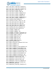
0.6 Feb 2018
Initial alpha release
- Updated Appendix
0.7 Jun 2018
Pin Cfg:
- VDDA pin on CSP package corrected in Pin List and Function Table
- DVDD pin added in BGA and CSP pkg diagrams and in Pin List and Function Table
I2C/SPI Master Module: Functional Description details added
ADC: ADC register set expanded to include DMA control/status registers
CTIMER: Corrected CTIMER Pad Input Connections table
GPIO: PADREGA corrected for SLMISO/SLMOSI function selections for PAD1 and PAD2
Electrical:
- Updated VESDCDM - ESD Charged Device Model (CDM)
- Updated VESDHBM - ESD Human Body Model (HBM)
- Updated Latch-up Current
0.8 Aug 2018
Package: CSP Package Drawing added
Appendix: Info0 information updated
Electrical: BLE specifications updated
0.9 Feb 2019
Pincfg: For CSP Pin Configuration Diagram and Pin List and Function Table, VSSB (C7) and
VDDBH_SW (C8) have been interchanged, CSP balls for GPIO4, 9, 10, 13, 14, 15, 21, 23,
24, 40 and 41 have been updated. Preliminary designation removed.
System Core (Flash): Updated note about allowable number of program cycles between
erase cycles.
Clock Gen: Clock tree diagram added.
Reset Module: Updated Block diagram for the Reset Generator Module
Electricals:
- ADC specifications updated
- Corremark current at 3.3V/48MHz corrected
0.9.1 TBD
MSPI: Pin Muxing table corrected
Ordering Information: CSP package added