
User Manual


Apollo3 Blue Datasheet
DS-A3-0p9p1 Page 88 of 909 2019 Ambiq Micro, Inc.
All rights reserved.
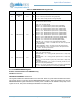
3.5.3.1.2.9ADCSTATUS Register
Power Status Register for ADC Block
OFFSET: 0x00000020
INSTANCE 0 ADDRESS: 0x40021020
This provides the power status for various blocks within the ADC. These status comes directly from the
ADC module and is captured through this interface.
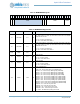
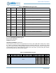
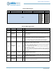
Table 21: SRAMCTRL Register
3
1
3
0
2
9
2
8
2
7
2
6
2
5
2
4
2
3
2
2
2
1
2
0
1
9
1
8
1
7
1
6
1
5
1
4
1
3
1
2
1
1
1
0
0
9
0
8
0
7
0
6
0
5
0
4
0
3
0
2
0
1
0
0
RSVD SRAMLIGHTSLEEP RSVD
SRAMMASTERCLKGATE
SRAMCLKGATE
RSVD
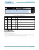
Table 22: SRAMCTRL Register Bits
Bit Name Reset RW Description
31:20 RSVD 0x0 RO
This bitfield is reserved for future use.
19:8
SRAMLIGHT-
SLEEP
0x0 RW
Light Sleep enable for each TCM/SRAM bank. When 1, corresponding
bank will be put into light sleep. For optimal power, banks should be put into
light sleep while the system is active but the bank has minimal or no
accesses.
ALL = 0xFF - Enable LIGHT SLEEP for ALL SRAMs
DIS = 0x0 - Disables LIGHT SLEEP for ALL SRAMs
7:3 RSVD 0x0 RO
This bitfield is reserved for future use.
2
SRAMMASTER-
CLKGATE
0x0 RW
This bit is 1 when the master clock gate is enabled (top-level clock gate for
entire SRAM block)
EN = 0x1 - Enable Master SRAM Clock Gate
DIS = 0x0 - Disables Master SRAM Clock Gating
1SRAMCLKGATE 0x0 RW
This bit is 1 if clock gating is allowed for individual system SRAMs
EN = 0x1 - Enable Individual SRAM Clock Gating
DIS = 0x0 - Disables Individual SRAM Clock Gating
0 RSVD 0x0 RO
This bitfield is reserved for future use.