
User Manual


Apollo3 Blue Datasheet
DS-A3-0p9p1 Page 82 of 909 2019 Ambiq Micro, Inc.
All rights reserved.
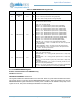
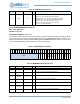
3.5.3.1.2.4MEMPWDINSLEEP Register
Powerdown SRAM banks in Deep Sleep mode
OFFSET: 0x0000000C
INSTANCE 0 ADDRESS: 0x4002100C
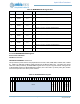
This controls the power down of the SRAM banks in deep sleep mode. If this is set, then the power for that
SRAM bank will be gated when the core goes into deep sleep. Upon wake, the data within the SRAMs will
be erased. If this is not set, retention voltage will be applied to the SRAM bank when the core goes into
deep sleep. Upon wake, the data within the SRAMs are retained. Do not set this if the SRAM bank is used
as the target for DMA transfer while CPU in deepsleep.
1PWRIOM0 0x0RW
Power up IO Master 0
EN = 0x1 - Power up IO Master 0
DIS = 0x0 - Power down IO Master 0
0PWRIOS 0x0RW
Power up IO Slave
EN = 0x1 - Power up IO slave
DIS = 0x0 - Power down IO slave
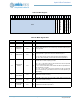
Table 13: MEMPWDINSLEEP Register
3
1
3
0
2
9
2
8
2
7
2
6
2
5
2
4
2
3
2
2
2
1
2
0
1
9
1
8
1
7
1
6
1
5
1
4
1
3
1
2
1
1
1
0
0
9
0
8
0
7
0
6
0
5
0
4
0
3
0
2
0
1
0
0
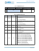
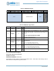
CACHEPWDSLP
RSVD
FLASH1PWDSLP
FLASH0PWDSLP
SRAMPWDSLP
DTCMPWDSLP
Table 14: MEMPWDINSLEEP Register Bits
Bit Name Reset RW Description
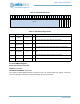
31
CACHEPWD-
SLP
0x0 RW
power down cache in deep sleep
EN = 0x1 - Power down cache in deep sleep
DIS = 0x0 - Retain cache in deep sleep
30:15 RSVD 0x0 RO
RESERVED.
14
FLASH1PWD-
SLP
0x1 RW
Powerdown flash1 in deep sleep
EN = 0x1 - Flash1 is powered down during deepsleep
DIS = 0x0 - Flash1 is kept powered on during deepsleep
Table 12: DEVPWREN Register Bits
Bit Name Reset RW Description