
User Manual


Apollo3 Blue Datasheet
DS-A3-0p9p1 Page 780 of 909 2019 Ambiq Micro, Inc.
All rights reserved.
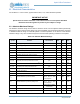
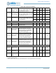
V
ADCIN_DIFF
Input voltage range in differen-
tial mode
-V
ADCREF
/
2
+V
AD-
CREF
/2 V
V
ADCINN
V
ADCINP
Absolute differential input volt-
age range
0 VDDH V
V
ADCREF_15E
External reference voltage
range (1.5v mode)
1.425 1.5 1.575 V
V
ADCREF_20E
External reference voltage
range (2.0v mode)
1.9 2.0 2.1 V
V
ADCREF_15I
Internal reference voltage range
(1.5v mode)
1.475 1.5 1.525 V
V
ADCREF_20I
Internal reference voltage range
(2.0v mode)
1.975 2.0 2.025 V
I
ADCIN
ADC channel pin input leakage
current (static)
GPIO 16 measured at 85 C,
TTT part, 2.05 V; 2 V on
pad; 10.8 nA with 3.63 or
1.8 V on VDD and pad
-.550nA
Z
ADC_CH0
ADC Channel 0 Input Imped-
ance
VDD = 3.63 V 360 720 kΩ
Z
ADC_CH1
- Z
AD-
C_CH7
ADC Channel 1 - Channel 7
Input Impedance
VDD = 3.63 V 180 3600 MΩ
C
ADCIN
Input source capacitance 4 pF
C
ADCVREF
External ADC capacitance for
internal reference
400 470 540 nF
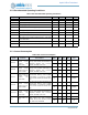
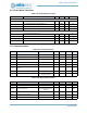
SAMPLING DYNAMICS
RES Resolution 8
14
bit
F
ADCONV
Conversion rate
1.2 (14b)
1.6 (12b)
2.0 (10b)
2.66 (8b)
MS/s
TTRIG_C-
START_REF0
Delay from cold start trigger to
start of scan, Internal Ref
652 µs
TTRIG_C-
START_REF1
Delay from cold start trigger to
start of scan, External Ref
137 µs
TTRIG_W-
START_LP1_RE
F0
Delay from warm start trigger to
start of scan, LPMODE1, Inter-
nal Ref
65.6 µs
TTRIG_W-
START_LP1_RE
F1
Delay from warm start trigger to
start of scan, LPMODE1, Exter-
nal Ref
1.52 µs
TTRIG_W-
START_LP0_RE
F0
Delay from warm start trigger to
start of scan, LPMODE0, Inter-
nal Ref
0µs
TTRIG_W-
START_LP0_RE
F1
Delay from warm start trigger to
start of scan, LPMODE0, Exter-
nal Ref
0µs
TSNGLSLOT_SC
NCMP_PM14
Delay from scan start to scan
complete, precision mode 14
40 cycles
Symbol Parameter Test Conditions Min Typ Max Unit