
User Manual


Apollo3 Blue Datasheet
DS-A3-0p9p1 Page 774 of 909 2019 Ambiq Micro, Inc.
All rights reserved.
21. Electrical Characteristics
For all tables T
A
= -40ºC to 85ºC, Typical values at 25ºC, 1.8v, unless otherwise specified.
IMPORTANT NOTICE
Specifications and other information in this advanced version of the Apollo3 Blue MCU
Datasheet should be regarded as preliminary and subject to change.
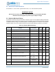
21.1 Absolute Maximum Ratings
The absolute maximum ratings are the limits to which the device can be subjected without permanently
damaging the device and are stress ratings only. Device reliability may be adversely affected by exposure
to absolute-maximum ratings for extended periods. Functional operation of the device at the absolute
maximum ratings or any other conditions beyond the recommended operating conditions is not implied.
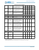
Table 1143: Absolute Maximum Ratings
Symbol Parameter Test Conditions Min Max Unit
V
DDP
Pad supply voltage - 3.63 V
V
DDH
Digital supply voltage - 3.63 V
V
DDA
Analog supply voltage - 3.63 V
V
IO
Voltage on all input and output pins 0 VDDH V
I
SRC_STD
Standard output pin source continuous current - 16 mA
I
SINK_STD
Standard output pin sink continuous current - 16 mA
I
HSC_PWR
High side power switch continuous source current
(1)
-50mA
I
HSP_PWR
High side power switch pulsed source current
(1)
10 ms pulse, 1% duty
cycle
-150mA
I
LSC_PWR
Low side power switch continuous sink current
(2)
-50mA
I
LSP_PWR
Low side power switch pulsed sink current
(2)
10 ms pulse, 1% duty
cycle
150 mA
T
S
Storage temperature -55 125 ºC
T
J
Junction temperature TBD 85.7 ºC
T
OP
Operating temperature -40 85 ºC
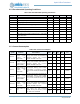
JA
Thermal resistance, junction to ambient
BGA Package on 4 layer
PCB in still air, 3mW
power dissipation
76.2 ºC/W
JC
Thermal resistance, junction to package case
BGA Package on 4 layer
PCB in still air, 3mW
power dissipation
17.0 ºC/W
T
REFLOW
Reflow temperature
Reflow Profile per JEDEC
J-STD-020D.1
260 ºC
I
LU
Latch-up current 100 mA
V
ESDHBM
ESD Human Body Model (HBM) 2000 V