
User Manual


Apollo3 Blue Datasheet
DS-A3-0p9p1 Page 764 of 909 2019 Ambiq Micro, Inc.
All rights reserved.
19. Voltage Comparator Module
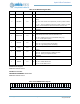
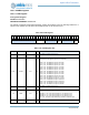
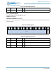
Figure 92. Block diagram for the Voltage Comparator Module
19.1 Functional Overview
The Voltage Comparator Module, shown in Figure 92, measures a user-selectable voltage at all times. It
provides interrupt and software access to the comparator output with multiple options for input and
reference voltages. It can be configured to generate an interrupt when the monitored voltage rises above a
user-configurable threshold or when the monitored voltage drops below a user-configurable threshold.
The voltage to be monitored is selected by programming the comparator’s positive terminal signal,
PSEL[1:0] and may be any of: 1) the supply voltage (VDDH), 2) the PTAT voltage from the temperature
sensor (VTEMP), or 3) two external voltage channels (CMPIN0 and CMPIN1).
The reference voltage is selected by programming the comparator’s negative terminal, NSEL[1:0] and may
be any of: 1) three external voltage channels (CMPRF0, CMPRF1, CMPRF2), or 2) the internally
generated reference (VREFINT). The internal reference voltage is tuned using an on-chip DAC with level
select signal LVLSEL[3:0]. When using external inputs or reference inputs, the associated pads must be
configured using the GPIO function selects explained in the GPIO document section.
The Voltage Comparator CMPOUT output will remain high while the voltage at the positive input is above
the voltage at reference input. The CMPOUT output will transition low when the voltage at the positive
input to the comparator falls below the reference input taking into account hysteresis (see Section 21.11 for
hysteresis range). The CMPOUT output is directly accessible by software by reading the CMPOUT field in
the status register. The OUTHI interrupt will be set if enabled and the CMPOUT transitions high or if it is
high at the time the interrupt is enabled. Similarly, the OUTLOW interrupt will be set if enabled and the
CMPOUT output transitions low or if it is low at the time the interrupt is enabled.
The Voltage Comparator Module is enabled by default and may be powered off by writing 0x37 to the
PWDKEY register
19.2 VCOMP Registers
Voltage Comparator
INSTANCE 0 BASE ADDRESS:0x4000C000
VDDH
DAC
VTEMP
CMPIN0
CMPIN1
CMPRF0
CMPRF1
CMPRF2
PSEL[1:0]
+
_
LVLSEL[3:0]
NSEL[1:0]
CMPOUT
POWER
DOWN
PWD