
User Manual


Apollo3 Blue Datasheet
DS-A3-0p9p1 Page 742 of 909 2019 Ambiq Micro, Inc.
All rights reserved.
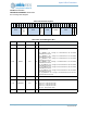
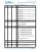
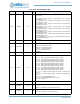
SL1CFG Register
Slot 1 Configuration Register
OFFSET: 0x00000010
INSTANCE 0 ADDRESS: 0x50010010
Slot 1 Configuration Register
11:8 CHSEL0 0x0 RW
Select one of the 14 channel inputs for this slot.
SE0 = 0x0 - single ended external GPIO connection to pad16.
SE1 = 0x1 - single ended external GPIO connection to pad29.
SE2 = 0x2 - single ended external GPIO connection to pad11.
SE3 = 0x3 - single ended external GPIO connection to pad31.
SE4 = 0x4 - single ended external GPIO connection to pad32.
SE5 = 0x5 - single ended external GPIO connection to pad33.
SE6 = 0x6 - single ended external GPIO connection to pad34.
SE7 = 0x7 - single ended external GPIO connection to pad35.
SE8 = 0x8 - single ended external GPIO connection to pad13.
SE9 = 0x9 - single ended external GPIO connection to pad12.
DF0 = 0xA - differential external GPIO connections to pad12(N) and
pad13(P).
DF1 = 0xB - differential external GPIO connections to pad15(N) and
pad14(P).
TEMP = 0xC - internal temperature sensor.
BATT = 0xD - internal voltage divide-by-3 connection.
VSS = 0xE - Input VSS
7:2 RSVD 0x0 RO
RESERVED.
1 WCEN0 0x0 RW
This bit enables the window compare function for slot 0.
WCEN = 0x1 - Enable the window compare for slot 0.
0 SLEN0 0x0 RW
This bit enables slot 0 for ADC conversions.
SLEN = 0x1 - Enable slot 0 for ADC conversions.
Table 1084: SL1CFG Register
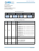
3
1
3
0
2
9
2
8
2
7
2
6
2
5
2
4
2
3
2
2
2
1
2
0
1
9
1
8
1
7
1
6
1
5
1
4
1
3
1
2
1
1
1
0
0
9
0
8
0
7
0
6
0
5
0
4
0
3
0
2
0
1
0
0
RSVD
ADSEL1
RSVD
PRMODE1
RSVD CHSEL1 RSVD
WCEN1
SLEN1
Table 1085: SL1CFG Register Bits
Bit Name Reset RW Description
31:27 RSVD 0x0 RO
RESERVED.
Table 1083: SL0CFG Register Bits
Bit Name Reset RW Description