
User Manual

Apollo3 Blue Datasheet
DS-A3-0p9p1 Page 739 of 909 2019 Ambiq Micro, Inc.
All rights reserved.
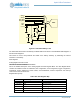
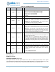
STAT Register
ADC Power Status
OFFSET: 0x00000004
INSTANCE 0 ADDRESS: 0x50010004
This register indicates the basic power status for the ADC. For detailed power status, see the power
control power status register. ADC power mode 0 indicates the ADC is in it's full power state and is ready
to process scans. ADC Power mode 1 indicates the ADC enabled and in a low power state.
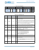
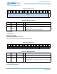
9:8 REFSEL 0x0 RW
Select the ADC reference voltage.
INT2P0 = 0x0 - Internal 2.0V Bandgap Reference Voltage
INT1P5 = 0x1 - Internal 1.5V Bandgap Reference Voltage
EXT2P0 = 0x2 - Off Chip 2.0V Reference
EXT1P5 = 0x3 - Off Chip 1.5V Reference
7:5 RSVD 0x0 RO
RESERVED.
4CKMODE 0x0RW
Clock mode register
LPCKMODE = 0x0 - Disable the clock between scans for LPMODE0. Set
LPCKMODE to 0x1 while configuring the ADC.
LLCKMODE = 0x1 - Low Latency Clock Mode. When set, HFRC and the
adc_clk will remain on while in functioning in LPMODE0.
3LPMODE 0x0RW
Select power mode to enter between active scans.
MODE0 = 0x0 - Low Power Mode 0. Leaves the ADC fully powered
between scans with minimum latency between a trigger event and sample
data collection.
MODE1 = 0x1 - Low Power Mode 1. Powers down all circuity and clocks
associated with the ADC until the next trigger event. Between scans, the ref-
erence buffer requires up to 50us of delay from a scan trigger event before
the conversion will commence while operating in this mode.
2RPTEN 0x0RW
This bit enables Repeating Scan Mode.
SINGLE_SCAN = 0x0 - In Single Scan Mode, the ADC will complete a sin-
gle scan upon each trigger event.
REPEATING_SCAN = 0x1 - In Repeating Scan Mode, the ADC will com-
plete it's first scan upon the initial trigger event and all subsequent scans will
occur at regular intervals defined by the configuration programmed for the
CTTMRA3 internal timer until the timer is disabled or the ADC is disabled.
When disabling the ADC (setting ADCEN to '0'), the RPTEN bit should be
cleared.
1 RSVD 0x0 RO
RESERVED.
0ADCEN 0x0RW
This bit enables the ADC module. While the ADC is enabled, the ADCCFG
and SLOT Configuration register settings must remain stable and
unchanged. All configuration register settings, slot configuration settings
and window comparison settings should be written prior to setting the
ADCEN bit to '1'.
DIS = 0x0 - Disable the ADC module.
EN = 0x1 - Enable the ADC module.
Table 1077: CFG Register Bits
Bit Name Reset RW Description