
User Manual

Apollo3 Blue Datasheet
DS-A3-0p9p1 Page 738 of 909 2019 Ambiq Micro, Inc.
All rights reserved.
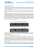
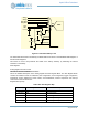
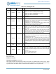
Table 1076: CFG Register
3
1
3
0
2
9
2
8
2
7
2
6
2
5
2
4
2
3
2
2
2
1
2
0
1
9
1
8
1
7
1
6
1
5
1
4
1
3
1
2
1
1
1
0
0
9
0
8
0
7
0
6
0
5
0
4
0
3
0
2
0
1
0
0
RSVD
CLKSEL
RSVD
TRIGPOL
TRIGSEL
RSVD
DFIFORDEN
RSVD
REFSEL
RSVD
CKMODE
LPMODE
RPTEN
RSVD
ADCEN
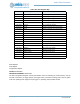
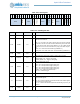
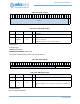
Table 1077: CFG Register Bits
Bit Name Reset RW Description
31:26 RSVD 0x0 RO
RESERVED.
25:24 CLKSEL 0x0 RW
Select the source and frequency for the ADC clock. All values not enumer-
ated below are undefined.
OFF = 0x0 - Off mode. The HFRC or HFRC_DIV2 clock must be selected
for the ADC to function. The ADC controller automatically shuts off the clock
in it's low power modes. When setting ADCEN to '0', the CLKSEL should
remain set to one of the two clock selects for proper power down sequenc-
ing.
HFRC = 0x1 - HFRC Core Clock divided by (CORESEL+1)
HFRC_DIV2 = 0x2 - HFRC Core Clock / 2 further divided by (CORESEL+1)
23:20 RSVD 0x0 RO
RESERVED.
19 TRIGPOL 0x0 RW
This bit selects the ADC trigger polarity for external off chip triggers.
RISING_EDGE = 0x0 - Trigger on rising edge.
FALLING_EDGE = 0x1 - Trigger on falling edge.
18:16 TRIGSEL 0x0 RW
Select the ADC trigger source.
EXT0 = 0x0 - Off chip External Trigger0 (ADC_ET0)
EXT1 = 0x1 - Off chip External Trigger1 (ADC_ET1)
EXT2 = 0x2 - Off chip External Trigger2 (ADC_ET2)
EXT3 = 0x3 - Off chip External Trigger3 (ADC_ET3)
VCOMP = 0x4 - Voltage Comparator Output
SWT = 0x7 - Software Trigger
15:13 RSVD 0x0 RO
RESERVED.
12 DFIFORDEN 0x0 RW
Destructive FIFO Read Enable. Setting this will enable FIFO pop upon read-
ing the FIFOPR register.
DIS = 0x0 - Destructive Reads are prevented. Reads to the FIFOPR register
will not POP an entry off the FIFO.
EN = 0x1 - Reads to the FIFOPR register will automatically pop an entry off
the FIFO.
11:10 RSVD 0x0 RO
RESERVED.