
User Manual

Apollo3 Blue Datasheet
DS-A3-0p9p1 Page 736 of 909 2019 Ambiq Micro, Inc.
All rights reserved.
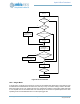
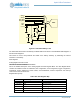
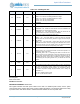
Figure 91. Switchable Battery Load
The switchable load resistor is enabled by the BATTLOAD bit as shown in the ADCBATTLOAD Register of
the MCUCTRL Registers.
This feature is used to help estimate the health of the battery chemistry by estimating the internal
resistance of the battery.
ADC Registers
Analog Digital Converter Control
INSTANCE 0 BASE ADDRESS:0x50010000
This is the detailed description of the Analog Digital Converter Register Block. The ADC Register Block
contains the software control for enablement, slot configuration, clock configuration, trigger configuration,
temperature sensor enablement, power modes, accumulate/divide, window comparison and interrupt
control for the ADC functional unit.
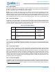
Register Memory Map
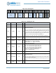
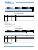
Table 1075: ADC Register Map
Address(s) Register Name Description
0x50010000 CFG Configuration Register
0x50010004 STAT ADC Power Status
0x50010008 SWT Software trigger
0x5001000C SL0CFG Slot 0 Configuration Register
0x50010010 SL1CFG Slot 1 Configuration Register
ADC
ADC_I0
...
ADC_I9
VDD
VSS
...
Temp Sensor
VIN
Select Ch 0xD
Input Voltage
BATTLOAD
R
on
≈ 500Ω
≈ 1/3
10KΩ
5KΩ
ADC_DIFF0
ADC_DIFF1