
User Manual


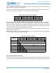

Apollo3 Blue Datasheet
DS-A3-0p9p1 Page 724 of 909 2019 Ambiq Micro, Inc.
All rights reserved.
▪ Window comparator for monitoring voltages excursions into or out of user-selectable thresholds
▪ Up to 2.67 MS/s effective continuous, multi-slot sampling rate
▪ Interrupts for FIFO full, FIFO almost full, Scan Complete, Conversion Complete, Window Incursion Win-
dow Excursion
18.2 Functional Overview
The Apollo3 Blue MCU integrates a sophisticated 14 bit successive approximation Analog to Digital
Converter (ADC) block for sensing both internal and external voltages. The block provides eight separately
managed conversion requests, called slots. The result of each conversion requests is delivered to a 16
deep FIFO. Firmware can utilize various interrupt notifications to determine when to collect the sampled
data from the FIFO. This block is extremely effective at automatically managing its power states and its
clock sources.
18.2.1 Clock Source and Dividers
The ADC runs off of the HFRC clock source. When the ADC block is enabled and has an active scan in
progress, it requests an HFRC clock source. There is an automatic hardware hand shake between the
clock generator and the ADC. If the ADC is the only block requesting an HFRC based clock, then the
HFRC will be automatically started. The ADC can be configured to completely power down the HFRC
between scans if the startup latency is acceptable or it can leave the HFRC powered on between scans if
the application requires low latency between successive conversions. The ADC supports 2 clock
frequency modes: 24MHz and 48MHz HFRC. 48MHz mode is the default mode of operation.
18.2.2 Channel Analog Mux
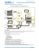
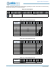
As shown in Figure 89, the ADC block contains a channel analog multiplexer on the input port to the
analog to digital converter. of the GPIO pins on the can be selected as analog inputs to the ADC through a
combination of settings in the PAD configuration registers in the GPIO block and settings in the
configuration registers described below.
The analog mux channels are connected as follows:
1. ADC_EXT0 external GPIO pin connection.
2. ADC_EXT1 external GPIO pin connection.
3. ADC_EXT2 external GPIO pin connection.
4. ADC_EXT7 external GPIO pin connection.
5. ADC_EXT8 external GPIO pin connection.
6. ADC_EXT9 external GPIO pin connection.
7. ADC_EXT_DIFF0P external GPIO connection (muxed with EXT8)
ADC_EXT_DIFF0N external GPIO connection (muxed with EXT9)
8. ADC_EXTDIFF1P external GPIO pin connection.
ADC_EXT DIFF1N external GPIO pin connection.
9. ADC_TEMP internal temperature sensor.
10. ADC_DIV3 internal voltage divide by 3 connection to the input power rail.
11. ADC_VSS internal ground connection.
EXT8-9 can be configured as a differential pair providing an additional differential pair or up to 2 single-
ended inputs from GPIO.
Refer to the detailed register information below for the exact coding of the channel selection bit field. Also
the use of the voltage divider and switchable load resistor are detailed below.