
User Manual


Apollo3 Blue Datasheet
DS-A3-0p9p1 Page 64 of 909 2019 Ambiq Micro, Inc.
All rights reserved.
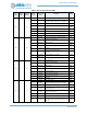
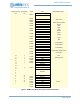
F5 - 45
0 UA1CTS UART1 Clear To Send (CTS) Input
1 NCE45
IO Master N Chip Select 45
Table 564, “NCE Encoding Table,” on page 382
Output
2CT22
Timer/Counter Interface Signal 22
See “Implementing Counter/Timer Connections” on
page 394.
Output
3 GPIO45 General Purpose I/O
Input/
Output
4 I2SDAT I2S Data Output
5 PDMDATA PDM Data Input
6 UART0RX UART0 Receive Input
7 SWO Serial Wire Debug Output Output
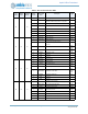
E7 - 46
0 I2SBCLK I2S Bit Clock Input
1 NCE46
IO Master N Chip Select 46
Table 564, “NCE Encoding Table,” on page 382
Output
2CT24
Timer/Counter Interface Signal 24
See “Implementing Counter/Timer Connections” on
page 394.
Output
3 GPIO46 General Purpose I/O
Input/
Output
4 SCCRST Secure Card Controller Reset Output
5 PDMCLK PDM Output Clock Output
6 UART1TX UART1 Transmit Output
7 SWO Serial Wire Debug Output Output
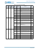
H9 G2 47
0 32kHzXT 32kHz Clock Output Output
1 NCE47
IO Master N Chip Select 47
Table 564, “NCE Encoding Table,” on page 382
Output
2CT26
Timer/Counter Interface Signal 26
See “Implementing Counter/Timer Connections” on
page 394.
Output
3 GPIO47 General Purpose I/O
Input/
Output
4RSVReserved
5 M5MOSI SPI Master 5 Output Data Output
6 UART1RX UART1 Receive Input
7RSVReserved
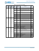
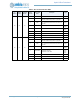
Table 1: Pin List and Function Table
BGA
Pin
Number
CSP Pin
Number
GPIO Pad
Number
Function
Select
Number
Pad Function
Name
Description Pin Type