
User Manual


Apollo3 Blue Datasheet
DS-A3-0p9p1 Page 637 of 909 2019 Ambiq Micro, Inc.
All rights reserved.
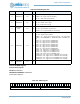
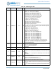
9TMRA6IE0 0x0RW
Counter/Timer A6 Interrupt Enable bit based on COMPR0.
DIS = 0x0 - Disable counter/timer A6 from generating an interrupt based on
COMPR0.
EN = 0x1 - Enable counter/timer A6 to generate an interrupt based on COM-
PR0.
8:6 TMRA6FN 0x0 RW
Counter/Timer A6 Function Select.
SINGLECOUNT = 0x0 - Single count (output toggles and sticks). Count to
CMPR0A6, stop.
REPEATEDCOUNT = 0x1 - Repeated count (periodic 1-clock-cycle-wide
pulses). Count to CMPR0A6, restart.
PULSE_ONCE = 0x2 - Pulse once (aka one-shot). Count to CMPR0A6,
assert, count to CMPR1A6, deassert, stop.
PULSE_CONT = 0x3 - Pulse continously. Count to CMPR0A6, assert,
count to CMPR1A6, deassert, restart.
SINGLEPATTERN = 0x4 - Single pattern.
REPEATPATTERN = 0x5 - Repeated pattern.
CONTINUOUS = 0x6 - Continuous run (aka Free Run). Count continuously.
ALTPWN = 0x7 - Alternate PWM
5:1 TMRA6CLK 0x0 RW
Counter/Timer A6 Clock Select.
TMRPIN = 0x0 - Clock source is TMRPINA.
HFRC_DIV4 = 0x1 - Clock source is the HFRC / 4
HFRC_DIV16 = 0x2 - Clock source is HFRC / 16
HFRC_DIV256 = 0x3 - Clock source is HFRC / 256
HFRC_DIV1024 = 0x4 - Clock source is HFRC / 1024
HFRC_DIV4K = 0x5 - Clock source is HFRC / 4096
XT = 0x6 - Clock source is the XT (uncalibrated).
XT_DIV2 = 0x7 - Clock source is XT / 2
XT_DIV16 = 0x8 - Clock source is XT / 16
XT_DIV128 = 0x9 - Clock source is XT / 128
LFRC_DIV2 = 0xA - Clock source is LFRC / 2
LFRC_DIV32 = 0xB - Clock source is LFRC / 32
LFRC_DIV1K = 0xC - Clock source is LFRC / 1024
LFRC = 0xD - Clock source is LFRC
RTC_100HZ = 0xE - Clock source is 100 Hz from the current RTC oscillator.
HCLK_DIV4 = 0xF - Clock source is HCLK / 4 (note: this clock is only avail-
able when MCU is in active mode)
XT_DIV4 = 0x10 - Clock source is XT / 4
XT_DIV8 = 0x11 - Clock source is XT / 8
XT_DIV32 = 0x12 - Clock source is XT / 32
RSVD = 0x13 - Clock source is Reserved.
CTMRB6 = 0x14 - Clock source is CTIMERB6 OUT.
CTMRA3 = 0x15 - Clock source is CTIMERA3 OUT.
CTMRB3 = 0x16 - Clock source is CTIMERB3 OUT.
CTMRA7 = 0x17 - Clock source is CTIMERA7 OUT.
CTMRB7 = 0x18 - Clock source is CTIMERB7 OUT.
CTMRB0 = 0x19 - Clock source is CTIMERB0 OUT.
CTMRB1 = 0x1A - Clock source is CTIMERB1 OUT.
CTMRB2 = 0x1B - Clock source is CTIMERB2 OUT.
CTMRB4 = 0x1C - Clock source is CTIMERB4 OUT.
BUCKBLE = 0x1D - Clock source is BLE buck converter TON pulses.
BUCKB = 0x1E - Clock source is Memory buck converter TON pulses.
BUCKA = 0x1F - Clock source is CPU buck converter TON pulses.
Table 912: CTRL6 Register Bits
Bit Name Reset RW Description