
User Manual


Apollo3 Blue Datasheet
DS-A3-0p9p1 Page 60 of 909 2019 Ambiq Micro, Inc.
All rights reserved.
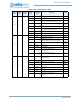
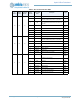
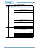
D5 - 31
0 ADCSE3 Analog to Digital Converter Single-Ended Input 3 Input
1 NCE31
IO Master N Chip Select 31
Table 564, “NCE Encoding Table,” on page 382
Output
2CT13
Timer/Counter Interface Signal 13
See “Implementing Counter/Timer Connections” on
page 394.
Output
3 GPIO31 General Purpose I/O
Input/
Output
4 UART0RX UART0 Receive Input
5 SCCCLK Secure Card Controller Clock Output
6 BLEIF_MISO BLE Interface MISO Observation Output
7 UA1RTS UART1 Request To Send (RTS) Output
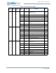
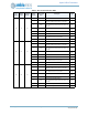
E6 - 32
0 ADCSE4 Analog to Digital Converter Single-Ended Input 4 Input
1 NCE32
IO Master N Chip Select 32
Table 564, “NCE Encoding Table,” on page 385
Output
2CT15
Timer/Counter Interface Signal 15
See “Implementing Counter/Timer Connections” on
page 394.
Output
3 GPIO32 General Purpose I/O
Input/
Output
4 SCCIO Secure Card Controller I/O
Input/
Output
5RSVReserved
6 BLEIF_MOSI BLE Interface MOSI Observation Output
7 UA1CTS UART1 Clear To Send (CTS) Input
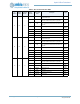
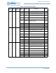
B6 - 33
0 ADCSE5 Analog to Digital Converter Single-Ended Input 5 Input
1 NCE33
IO Master N Chip Select 33
Table 564, “NCE Encoding Table,” on page 382
Output
2 32kHzXT 32kHz Clock Output Output
3 GPIO33 General Purpose I/O
Input/
Output
4 BLEIF_CSN BLE Interface Chip Select Observation Output
5 UA0CTS UART0 Clear To Send (CTS) Input
6CT23
Timer/Counter Interface Signal 23
See “Implementing Counter/Timer Connections” on
page 394.
Output
7 SWO Serial Wire Debug Output SWO
Table 1: Pin List and Function Table
BGA
Pin
Number
CSP Pin
Number
GPIO Pad
Number
Function
Select
Number
Pad Function
Name
Description Pin Type